Introduction: PCB Milling Using a 3D Printer


I've made a number of projects and Instructables with electronic circuits. And most of them used a prototyping PCB. This works fine, and it's a quick way to finish a project. But creating a PCB yourself gives a project a more professional appearance. It looks less messy, and reduces the chance of faults and defects. That is why I started researching how to make PCBs.
It has been a few decades since I have designed and etched my last PCB. And for some future projects, I want to make small PCBs myself. These will not be complex, just one or two layers. And I would rather not use any chemicals. That is why I decided to make PCBs using a CNC machine.
I have some experience with hand routers, and I've made a drone frame with a dremel router once. Unfortunately this router isn't accurate enough to make PCBs.
I also have experience with 3D printers. My previous Instructable was about creating and improving an Anet A8 3D printer.
In this Instructable I combine these two items: Controlling a dremel with an Anet A8 printer. This won't be a fast and very strong CNC machine, but it should be capable of making PCBs.
I usually make the design of an electrical diagram on paper. And after some iterations this results in a workable schedule for a prototype PCB.
This instructable uses the Autodesk Eagle PCB design tool. I started with the Circuit Board Design Class. In this course an electrical diagram is made in Autodesk Eagle (lesson 2). This is converted into a PCB design (lesson 3). And from this point the course continues with selecting a manufacturer for the PCB.
This instructable replaces step 3. I'll be my own manufacturer, making the PBC. This reduces cost, and I don't have to wait a few days for my PCB to arive.
Step 1: Sample Schematic


The sample project in this Instructable is a PCB board for a Cherry keys tester. These 9 keys will be connected just like a 4 x 4 keyboard module.
All keys are placed in a matrix, and it requires some software (or library) to read the keys with an Arduino. I've made a 4 x 4 example on Tinkercad. The code isn't optimized, which makes it very readable. All input pins are defined as INPUT_PULLUP. They always return TRUE (1) unless they are connected to the GND or a LOW (output) pin. The program starts with setting pin 5 to LOW. This makes it possible to measure all values of the four buttons in row 1. And continues with the other rows.
It is posible to press multiple buttons at the same time. And the program returns a value for each button. But there is one problem with some combinations. Pressing three buttons might result in detecting 4 buttons. This is called ghosting and can be solved by adding a diode for each button.
The choice of a keypad with Cherry keys has been a good choice for this Instructable.
First, the keys must have exactly the same distances apart. With a handmade PCB (etching and drilling) these holes will never be exactly in the right place. And with a keyboard you want the keys to be exactly aligned. Otherwise, it looks messy.
Secondly, it showed some 'problems' which would not have happened with regular components. These keys have a mount point for exact positioning. This requires a hole with a diameter of 4 mm. And the dremel can't handle 4 mm tools. In addition to etching and drilling, it is therefore also necessary to mill.
Step 2: Fusion 360 Gcode


The sample schematic is very simple. It can easily be made with Fusion 360. However, all components/holes and traces must be created manually. And this is hard to manage for large/complex PCBs.
There are two Instructables which explain how to "get started with CNC" with fusion 360. And I've managed to create a PCB and convert it to a GCode file. This is a file which contains all instruction for the 3D printer:
(keypad)
(Machine)
(  vendor: SNAPMAKER)
(  description: Generic Snapmaker Marlin v20180725)
M3
G4 S2
G21
G90

(2D Adaptive4)
G0 X-79.843 Y-81.637 Z15.000
G0 X-79.843 Y-81.637 Z15.000
G0 X-79.843 Y-81.637 Z5.000
G0 X-79.843 Y-81.637 Z0.160
G1 X-79.843 Y-81.637 Z0.080 F60
G1 X-79.842 Y-81.631 Z0.049 F60
G1 X-79.838 Y-81.614 Z0.023 F60
This GCode, made with Fusion 360, can be modified to be used with my Anet A8 3D printer. The first eight lines (header) must be modified. But the lines starting with G0 and G1 contain all required movements for the 3D printer.
An online simulation shows the toolpath for this PCB. And most time is used for milling to remove copper. It would save a lot of time when the copper parts in the design are enlarged. Or by adding a ground (GND) which is conneced to large copper planes on the board. This file made with Fusion 360 isn't perfect. But, with some changes, it can be used to create a PCB.
I haven't used the Fusion 360 output to create a PCB. But this example shows the workflow of making a PCB with a CNC machine:
- Create a schematic.
- Design the PCB layout.
- Create 3 different milling operations: Etching, drilling and milling.
- Convert the 3 milling operations to Gcode files.
- Adjust the Gcode files for the 3D printer.
- Place the PCB on the printer.
- Adjust the starting point of the printer.
- Turn on the dremel.
- Upload the Gcode files to the printer.
Attachments

Step 3: Dremel Holder


The 3D printer used in this Instructable is an Anet A8. This is a cheap Prusa based 3D printer (about €130, $150) with which you can make fine 3D prints. How to build and improve this printer is described in my previous Instructable: "Buid and Improve a 3D printer".
This dremel holder is made for the "Dremel 225-01 Flex Shaft Attachment". This fits all dremels, and ensures that less weight is attached to the X axis. If you have another brand multi tool, you can easily design and print a holder yourself.
Remove the heatbed and replace it with a piece of MDF with the same size. The PCB will be attached to this plate with double-sided adhesive tape. The advantage of MDF is that it is flat. You can place the MDF on top of your heatbed, but make sure you don't drill into your heatbed!
Remove the extruder, the fan and the metal extruder carriage. And attach the dremel to the 3 linear guides for the X axis.
Disconnect the headbed, thermistors, fans and extruder from the heatbed. Leave the end-stops and X,Y and Z-motors connected and place the Z endstop at the maximum height. Keep the LCD screen connected, to load GCode files from the SD card.
These steps have turned your printer into a CNC machine. With the accompanying benefits and dangers.
Do not home your printer until you have adjusted the Z axis endstop.


Step 4: Autodesk Eagle


Autodesk Eagle can be used to design electrical diagrams. The software is free for DIY projects, and can handle PCBs up to 80 cm2.
Installing the Eagle software is easy. Installing the library and the gcode plugin is also easy. To do this, certain files must be placed in certain folders after installation of the Eagle software: Place all libraries in the "libraries" folder and extract the pcb-gcode-archive in the "ulps" folder.
I have made some adjustments in the Cherry library and some other default Eagle libraries.
I'm using a 0.8 mm cutter to create the PCB. As a result, the mimimum distance between the copper paths is also 0.8 mm. And I don't plan to replace the tool while making the PCB: All component holes will be at least 0.8 mm.
The standard Eagle libraries contains components with a thinner hole diameter. With the corresponding pads. However, these pads are too small for the 0.8 mm cutter/drill. So I adjusted the pads of all components used on this PCB. I gave them a diameter of 3 mm, with a hole of 0.8 mm.
Step 5: Eagle Libraries


There are two types of Cherry keys: PCB and housing mounted. The PCB (direct) mounted versions have three mounting pins and are only available from Cherry itself. The general available housing version has only one mounting pin.
The Eagle Cherry library only contains the PCB version with 3 holes. You can modify the library file with a text editor, or by altering the library in Eagle itself.
<library>
<packages>
<package name="CHERRY_MX">
<description>Cherry keymodule MX
Default shape</description>
<hole x="-5.08" y="0" drill="1.7"/>
<hole x="5.08" y="0" drill="1.7"/>
<pad name="S1" x="-3.81" y="2.54" drill="1.5" diameter="2.54"/>
<pad name="S2" x="2.54" y="5.08" drill="1.5" diameter="2.54"/>
<hole x="0" y="0" drill="4.1"/>
Open the cherry.lbr file in Eagle (libraries > libraries > double click on "cherry.lbr"). Double click on the CHERRY_MX footprint to open an editor to adjust the footprint.
This file contains several layers, and the holes are placed on layer 44 (drills). I've removed all three mount points, and added a milling operation for the 4 mm hole in the center. The two pads are enlarged and modified for the drilling bit.
I've also modified the diode (1N4148), resistor (0204/7) and pinheader (3 and 4 pins) libraries. All pads are enlarged to 3 mm with a 0.8 mm hole.
Copy all files from the zipfile to the libraries folder in the Eagle documents directory. All four libraries must be enabled (Library > Open Library manager > Available Tab > Cherry > Use), which is indicated by a green dot.
Attachments

Step 6: Eagle Schematic

The first step in the Eagle software is to create the schematic. Use the components from the modified libraries and arrange them on the screen. Use the net (green line) tool to connect the components. Don't use the draw tool for this.
I've modified the sample schematic to prevent ghosting. The three resistors are optional, and can be used as pull up/down resistor.
Give all parts a logical name. Press the "generate/switch to board" button when the schematic is finished.
Attachments
Step 7: Eagle Board


The Eagle PCB design shows the PCB from the frontside. And the axis (0,0) is located at the left bottom of the design.
All keys are placed on a 20 x 20 mm raster. Use the properties (i) tool to position all objects (s1 = 20,60 ; s2 = 40,60 ; s3 = 60,60 ; s4 = 20,40 ; s5 = 40,40 ; s6 = 60,40 ; s7 = 20,20 ; s8 = 40,20 ; s9 = 60,20 ). The milimeters are automaticly converted to mill (one thousandth of an inch).
Choose a logical location for the diodes, resisors and pins.
The yellow lines are the signal wires. These must be replaced by routes. These routes can be placed on the Top (layer 1, red) or bottom (layer 16, blue). Only the blue lines will be 'etched' by the dremel. Both layers can be connected by a 'Via', but this results in a wire bridge.
Each element must have a property. I've altered all resistors to 10K Ohm (property/info screen).
This board can be made on one layer without air wires. I have chosen to use some wire bridges.
Attachments
Step 8: PCB Manufacturing

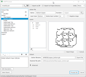
This is the next step to create the PCB. Pressing the "Manufacturing" button opens a preview window. This window shows both sides and all drills (top side only).
The PCB design must be saved in a readable format before it can be processed further. This is done with the CAM-processor. I've used the default values, and processing creates two folders in the project folder:
Drillfiles:
- drills.xln
GerberFiles:
- copper_bottom.gbr
- copper_top.gbr
- gerber_job.gbrjob
- profile.gbr
- silkscreen_bottom.gbr
- silkscreen_top.gbr
- soldermask_bottom.gbr
- soldermask_top.gbr
- solderpaste_bottom.gbr
- solderpaste_top.gbr
These files can be send to a PCB manufacturer. This board can be manufactured for about $10. With about $10 shipping costs.
A 15 x 20 cm blank PCB is about €1.50 at Alieexpress. Shipping included (14-21 days).
These Gerber files can't be used with the Anet A8 printer. But it's posible to use these files to create the required files. All generated files are textfiles and contain X and Y positions for all copper traces, solder masks and drills.
Attachments
Step 9: Gcode

The 3D printer firmware uses Gcode to control the printer. When creating a 3D print, this code is created during the slicing of the STL file. This Gcode file contains all commands to control the electronic parts. It is a readable textfile with a fixed format:
- Header
- Layer 1
- Layer 2
- ...
- Layer N-1
- Layer N
- Footer
All X, Y and Z coordinates in the gcode file are absolute. The Home position equals (0,0,0) and the middle of the heatbed equals (110,110,0).
It is possible to connect the 3D printer to a computer by USB and send GCode commands to the printer.
I'm using Pronterface for a while to test 3D printers. It's easy to install and use, but it's getting old. The latest version is from november 2017. Download the file and extract all files to a folder (no need for installation). There is a command line and graphical version. Start pronterface.exe for the graphical version. Connect the printer with an USB cable. Select the com port (eg com4) and a bautrate of 115200 and press the connect button. There are 4 home buttons: Start with the Y axis, then the X axis and finally the Z axis.
The box near the "Send" button is used to enter Gcode which will be executed by the printer. Some important gcodes are:
G21 = set units to mm
G28 = move to home
G90 = absolute
G00 = fast position
G01 = normal move
M114 = show current position
Start with the following commands (one by one):
- G28
- G21
- G90
- G1 Z50 F600
- G1 X100 Y100 F600
- M114
This moves the dremel 5 cm above the home position. The last command moves the dremel almost to the middle of the working area. The M114 command gives the current position: X:100.00 Y:100.00 Z:50.00 E:0.00. The idea is to place the toolhead to the exact start position (with pronterface) and make this the new home position (0,0,0):
G92 X0 Y0 Z0
This command makes the current positon (100,100, 50) the new home position (0,0,0). And the following command move the toolhead to a location, and back to this initial (new home) position:
G1 X10 Y10 F600
G1 X0 Y0 F600
The 3D printer doesn't allow negative postions until the software endstops are disabled:
M211 S1 (disable software endstop)
This allows the toolhead to move to any position! The hardware endstops are still enabled, but there are only 3 of them.
At this point it's posible to load the Fusion 360 GCode file and execute the Gcode commands. This doesn't have to be a PCB.
The Gerber files from the Eagle software must be converted to Gcode files. I found two programs to make this conversion:
The first program is an add-on to the Eagle software. And the other program is a stand alone program which converts Gerber files to Gcode files.
Step 10: PCB-GCode


PCB-GCode is an "user language program" for the Eagle software. It contains two programs: pcb-gcode and pcb-gcode-setup. Download the "pcb-gcode-3.6.0.4.zip" file and extact all files in the ulps folder of the Eagle directory.
Open the PCB and press the ULP button. Now select the ulps-folder instead of the examples folder and start with opening the setup file. The Anet a8 requires the "generic.pp" setup file.
All other settings depend on the mill size and board height. The sample settings are for a 0.8 mm mill and a 1.6 mm PCB board.
The generated GCode files contains negative X values. Both axis (X, Y) of the bottom etch/drill files start in the lower right corner. This is shown in the viewer image (crosshair on second image).
The file can be opened and altered by a text editor:
(Current profile is .../EAGLE/ulps/profiles/generic.pp  )
G21
(Absolute Coordinates)
G90
G00 X0.0000 Y0.0000
M03
G04 P3.000000
G00 Z2.5000
G00 X-38.1154 Y69.8738
G01 Z-0.2000 F100.00
G01 X-38.1154 Y70.1262 F100.00
G01 X-38.0825 Y70.3764
G01 X-38.0171 Y70.6202
G01 X-37.9205 Y70.8534
G01 X-37.7943 Y71.0720
G01 X-37.6407 Y71.2722
G01 X-37.4622 Y71.4507
The GCode files made with this tool don't have any mill code. It looks like it doesn't read layer 46 (milling).
Attachments
Step 11: PCB2GcodeGUI


The PCB2GcodeGUI-tool uses the Gerber files which are made by the Eagle software. And it requires 3 or 4 files:
- copper_top.gbr (optional)
- copper_bottom.gbr
- profile.gbr
- drills.xln
These files are converted to 4 gcode files (NCG-extension):
- back
- drill
- front
- outline
The back, drill and outline files are required for this PCB. Uploading these files to a GCode viewer shows the toolpaths for these GCode files.
The PCB2GcodeGUI files contain GCode which isn't compatible with the Anet A8 printer. The orginal output contains some invalid commands:
G00 X31.89760 Y8.87778 ( rapid move to begin. )
F50.00000
G01 Z-0.05000
G04 P0 ( dwell for no time -- G64 should not smooth over this point )
F100.00000
X31.89760 Y8.87778
X31.89760 Y15.41648
X31.97830 Y15.51917
...
X36.39929 Y8.80006
X36.25177 Y8.85287
X36.05759 Y8.87778
X31.89760 Y8.87778
G04 P0 ( dwell for no time -- G64 should not smooth over this point )
G00 Z5.00000 ( retract )
All lines which start with F or X must be altered:
G00 X31.89760 Y8.87778 ;( rapid move to begin. )
G01 F50.00000
G01 Z-0.05000
;G04 P0 ;( dwell for no time -- G64 should not smooth over this point )
G01 F100.00000
G01 X31.89760 Y8.87778
G01 X31.89760 Y15.41648
G01 X31.97830 Y15.51917
...
G01 X36.39929 Y8.80006
G01 X36.25177 Y8.85287
G01 X36.05759 Y8.87778
G01 X31.89760 Y8.87778
;G04 P0 ;( dwell for no time -- G64 should not smooth over this point )
G00 Z5.00000 ;( retract )
This can be done with a regular text editor (Ultraedit). Save the altered files as .GCode files.
Attachments
Step 12: GCode Difference

The two methods in the previous steps give different outputs. Both methods can't be combined directly for a single PCB. The Eagle Gcode files uses negative values for the X coordinates and the PCB2GcodeGUI uses positive values for the X coordinates. The image shows the result of both operations without any modifications.
To combine the files, the cnc tool must be repositioned before executing each GCode file.
Zooming with the GCode viewer shows small differences between both etch files.The Eagle GCode makes larger pads and thicker copper traces. But it doesn't mill the 9 holes for the keys, and cuts the outline in a single pass.
The PCB2GCode files mills the 9 holes and outline in steps of 0.2mm.
Step 13: Tools & Speed


I've bought some PCB mills at Aliexpress. These are 0.8 mm thick with a shank diameter of 3.75 mm.
The feedrade for these small mills should be about 1% of the diameter per revolution. These bits might break when moving at higher speeds. And milling at slower speed will wear the bit faster.
The dremel 4000 has a speed between 5000 and 35000 rpm. Running at half speed with flexible shaft gives about 17.000 rpm.
The sample GCode files use a speed of 100 mm/min. And 100/17,000 = 0.0058 mm. This is the removed material at a single rotation.
The rule of thumb equals 1% of 0,8 mm = 0,008 mm. The current speed should be fine.
Step 14: First Test

This first test has been made with an early version of the Eagle etch file with soft plastic.
Use double sided adhesive tape to attach the PCB. It is important to level the bed with the PCB attached. I've used the same method as leveling a 3D printer. Use a sheet of paper, and level the bed at 4 points. This will be the Z=0 height.
Move the milling tool to the start position with the milling tool just above the PCB (one sheet of paper, Z=0). This will be the new home position. The Eagle GCode file starts at the right lower corner, and the PCB2GcodeGUI file starts at the left lower corner.
Start with the following GCodes:
G21
G90
G92 X0 Y0 Z0
M211 S1
Then remove the header from the etch-file and load it with Pronterface. Press print to execute all commands after starting the Dremel tool.
Step 15: Mill Size

I've choosen to use a 0,8 mm mill. This makes it possible to make this simple PCB. The GCode viewer and Machine code simulator has been used to show the toolpath for the etch-operations before. And it shows all milling operations for the PCB.
At some points the diameter of the 0.8 mm mill is too large. The default resolution for the pin headers is 2.54 mm (1/10 inch). This is the distance between the holes in a prototyping PCB board. A 0.8 mm mill leaves 1.75 mm for the pad. And a hole of 0.8 mm will be drilled in the middle of this pad. Leaving 0.5 mm on the short side, and 1 mm on the long side.
For more complex PCBs, it is probably better to choose a smaller cutting diameter.
Step 16: Combined GCode

Both tools create several GCode files. And these can be combined to a single GCode file.
A regular GCode file contains a header, all layers and a footer.
I'll use the etch and drill file from the Eagle GCode file combined with the modified outline file from PCB2GcodeGUI:
- Keypad CNC.bot.etch
- Keypad CNC.bot.drill
- outline
The header and footer of each file is removed. The combined file gets the following header:
G21
G90
G92 X0 Y0 Z0
M211 S1
The tool must be placed at the starting point and this will be the (0,0,0) position.
The content of the etch file is placed after the header:
G00 Z2.5000
G00 X-38.1154 Y69.8738
G01 Z-0.2000 F100.00
G01 X-38.1154 Y70.1262 F100.00
G01 X-38.0825 Y70.3764
G01 X-38.0171 Y70.6202
G01 X-37.9205 Y70.8534
...
...
G01 X-68.7278 Y54.7393
G01 X-68.9280 Y54.5857
G01 X-69.0746 Y54.5010
G01 X-69.0746 Y52.6033
G01 X-67.3967 Y50.9254
G01 X-61.6890 Y50.9254
G01 X-61.6043 Y51.0720
G00 Z2.5000
Followed by the drill file:
G00 Z2.5000
M03
G04 P3.000000
G00 X-36.1900 Y42.5400
G01 Z-1.6250 F100.00
G00 Z2.5000
G00 X-36.1900 Y5.0000
G01 Z-1.6250 F100.00
G00 Z2.5000
...
...
G00 Z2.5000
G00 X-30.0000 Y23.8100
G01 Z-1.6250 F100.00
G00 Z2.5000
G00 X-30.0000 Y30.0000
G01 Z-1.6250 F100.00
G00 Z2.5000
The PCB2GcodeGU file uses positive value for the X asix. This requires a repositoning of the X axis:
G01 X-80.0000 Y0.0000 F100.00
G01 Z0.0000 F100.00
G92 X0 Y0 Z0
This moves the tool 80 mm (PCB size, always check this new position). And redefines the zero position for the final part.
This file mills the holes.
G00 X5.38760 Y3.93573 ( rapid move to begin. )
G01 Z-0.18056 F50.00000 ( plunge. )
G04 P0 ( dwell for no time -- G64 should not smooth over this point )
G01 F100.00000
G01 X5.38760 Y3.93573
G01 X5.02587 Y4.08442
G01 X4.69801 Y4.30241
...
...
G01 X75.42624 Y77.77699
G01 X75.81293 Y77.84488
G01 X76.00887 Y77.85006
G01 X76.21263 Y77.83497
G01 X76.58578 Y77.75133

G04 P0 ( dwell for no time -- G64 should not smooth over this point )
G00 Z10.000 ( retract )
The file should end with a footer (End program):
M2
This combined file can be used to make the PCB with a 3D printer.
This is the GCode for a single sided PCB. It is posible to create a double sided PCB, but this requires 2 GCode files: One for each side.
I would start with the top side, and drill two holes at two (or four) corners of the PCB (0,0 and 80,80) just before etching the topside. These additional holes can be used to align the board for the bottom side.
And draw horizontal lines on the print bed to facilitate repositioning.
Step 17: First PCB

The first PCB failed for two reasons. First, the mill wasn't close enough onto the PCB in two corners: The mill must be placed just above the copper layer.
You can use a multimeter to measure the height. Move the toolhead down very slowly. And stop if the resistance between the tool and the PCB equals 0 Ohm.
Or turn on the dremel and move the toolhead down very slowly. And stop as soon as the mill removes some material.
Secondly, the first move command didn't work as expected: Normally the Anet A8 homes to (0,0,0) by usage of the end switches. Then it moves to it's initial position above the heatbed and sets this position to (0,0,0).
This initial homing is also executed when I start my custom GCode file. It moved the entire PCB 30 mm on the x-axis and 10 mm on the y-axis.
But it's only executed once (after turning on/reset) and this can be solved by a change in the workflow:
- Place the PCB on the printbed
- Turn on the printer
- Home X, Y and Z to the printers home position
- Insert the mill
- level the printbed at all corners of the PCB (Multimeter)
- Move the toolhead to the initial position: just above the PCB (Multimeter)
- Mark this as home (G92 X0 Y0 Z0)
- Turn on the dremel
- Load and execute the etch GCode file from the SD card
- Optionally change the home position
- Load and execute the drill GCode file from the SD card
- Optionally change the home position
- Load and execute the mill GCode file from the SD card
- Move the toolhead up
- Turn off the dremel
- Remove the mill
- Remove the PCB from the heatbed
- Turn off the printer
It's even posible to alter the mill between the GCode files. The printer remembers the home position, even after moving the toolhead by the menu.
Step 18: Second PCB


In the second attempt, I 'printed' the individual files separately. Using the workflow of the previous step. This gave an usable PCB:
The Cherry keys require a 0,059 inch (1.5 mm) hole for the pins. And I've used a 0.0320 inch (0.8 mm) tool. This can be solved by adding these holes to the milling GCode file. Or by changing the tool while drilling the PCB. I only ordered some 0.8 mm mills, and have to order different sizes for my next PCB.
The second part which went wrong are the 9 holes for the keys. They were only 2.8 mm instead of 4 mm. This was caused by a setting in PCB2Gcode.
The GCode shows the position and the dimensions. For example:
G01 X40.96405 Y39.85082
G01 X40.40787 Y40.01950
G01 X40.13213 Y40.29537
G01 X39.98283 Y40.65600
G01 X39.96363 Y40.85052
G01 X39.98285 Y41.04592
G01 X40.40797 Y41.68209
G01 X40.76837 Y41.83144
G01 X40.96334 Y41.85072
G01 X41.15829 Y41.83157
G01 X41.88773 Y41.23261
G01 X41.96352 Y40.85115
G01 X41.94437 Y40.65567
G01 X41.88790 Y40.46929
G01 X41.34511 Y39.92649
The X and Y movements are from 39.96363 to 41.96352 (X) and from 41.85072 to 39.85082 (Y). A distance of 1.999 mm. And 0.8 mm for the tools gives a total size of 2.8 mm.
This hole was defined in the Cherry library as a 63 mill (1,6 mm) radius and a 31.5 mill (0,8 mm) width.
1.6 + 1.6 + 0.8 should give 4 mm. But the PCB2GcodeGUI GCode file made this a 2.8 mm hole.
The gerber file gives the folowing boundaries for this center hole:
X384000Y400000D02*
X416000Y400000D01*
X400000Y416000D01*
X400000Y384000D01*
These values should give a 3.2 mm hole. And tool should add 0,8 mm for a 4 mm hole.
The Outline "Edge line width" setting in PCB2GcodeGUI influences the size of these holes. It creates a 3.2 + 0.8 mm hole when set at 0.8. And I've used the value of 0.4 mm for this PCB.
Both 'problems' are solved by manually drilling larger holes. I had already removed the PCB from the board.
At this point I've managed to make a PCB with my 3D printer. The next step is to clean the board and solder some Cherry keys and diodes.
Attachments
Step 19: (Large PCBs)


The free version of eagle allows for boards up to 80cm2 (about 9 x 9 cm). Larger PCBs require a subscription. It is posible design two PCBs in Eagle and 'etch/mill' them on a single PCB. It requires exact postioning before starting the second GCode-file, but this is a method to make a large PCB.
This method is requires multiple schematics. And this increases the chance of mistakes.
The Anet A8 printbed limits the PCB size to to 22 x 22 cm (484 cm2). About 6 times the maximum PCB size of 80 cm2. This is too small for a regular keyboard. But sufficient for an Ergodox style keyboard. It requires about 4 different PCB designs combined into a single GCode file.
By designing the PCB at a half scale (50%), all the advantages of Eagle are retained. A single schematic, and a single PCB design. This requires a custom library with Cherry Keys at half the original size. This can be done with usage of a few different components (one type resistor, switch and diode). And all traces must be at half the thickness.
It takes a 3D printer firmware modification before this 50% GCode files can be used. The stepsize of the stepper drivers must be adjusted by 2 (for X and Y). This will translate the 80 x 80 cm board (at 50%) to a 160 x 160 cm board.
For a single DIY project this can be done, but it's not practical for an Instructable project.
After some research and experimenting, I managed to make a PCB with an Anet A8 3D printer. And after some practice it should be possible to make double-sided PCBs. With these it is especially important to calibrate the starting position properly.
Although the process seems complicated, it has the advantage that no chemicals are used. I am therefore satisfied with the end result, and will create a PCB with this method more often in the future.
Gosse Adema

Second Prize in the
PCB Contest