

Introduction: Build Custom ESP32 Boards From Scratch! | the Complete Guide to Designing Your Own ESP32-S3 and C3 | Full Tutorial


In this article, I will teach you everything you need to start designing your own custom ESP32 microcontrollers for your projects. This will include the complete build of the popular ESP32-S3 and C3.
For the best quality read, check out this article on my homepage here. If there's a pop-up, just simply click dismiss at the bottom. Also, don't forget to subscribe for free to support my work! :)
Step 1: A Quick Preview
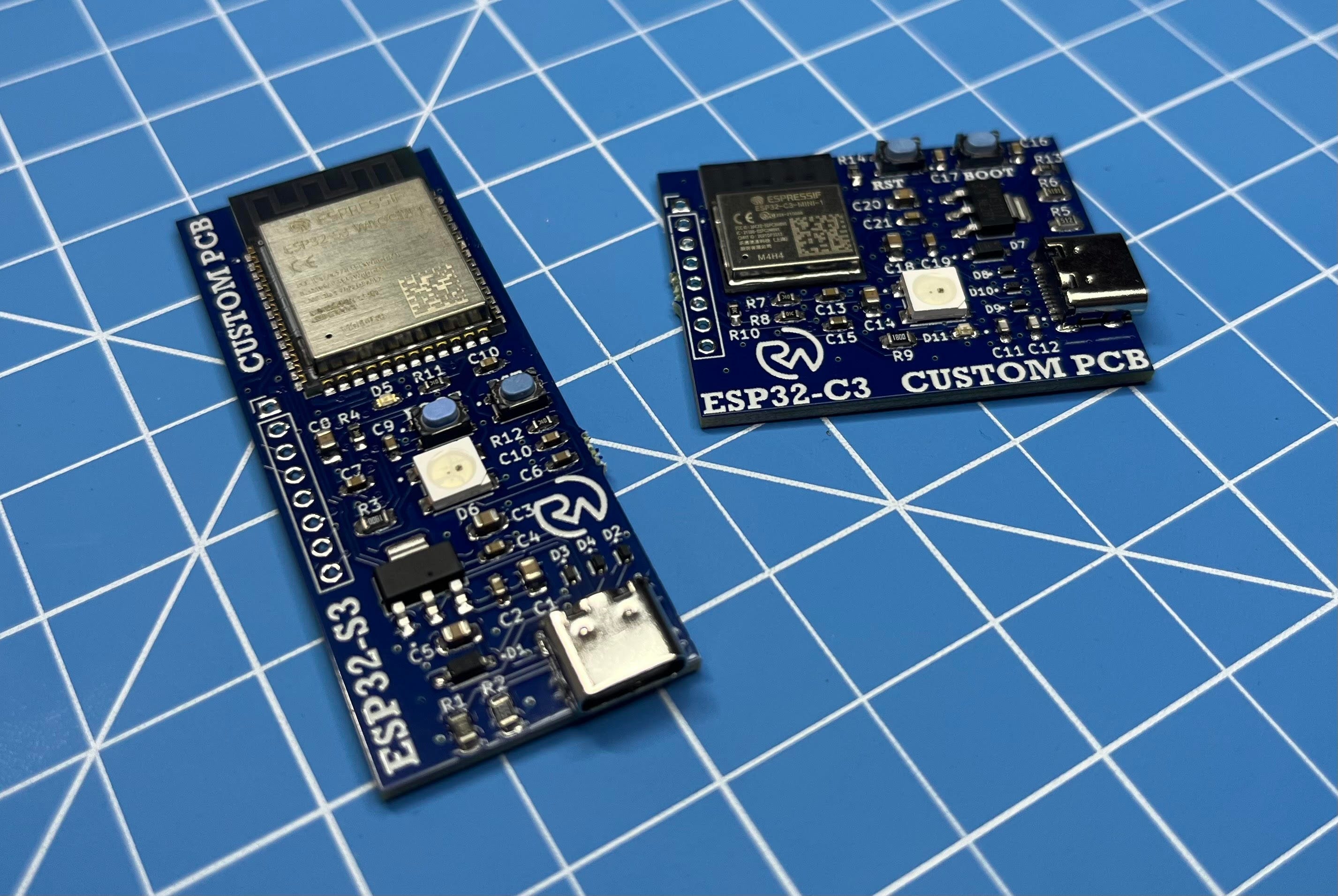
These are the ESP32 microcontroller boards I use in almost every project. The benefit of making them over buying commercial DevKits is that they are custom, meaning you can fit precise components for specific applications in the least amount of space possible.


In this article, instead of a project like I normally do, I thought it would be a good idea to get down into the specifics of how exactly these microcontroller boards are built and show you every step of their design process. This way, you can build them for yourself with confidence in the future and never shy away from “complex” circuitry again. It’s really not as difficult as it may seem!
Plus, they can do so many amazing things! (Besides controlling every project I’ve ever made.) For example, here’s a cool little demo video of these boards controlling a TFT display via SPI communication (which I’ll also explain how to set up in this article).
Step 2:

In this tutorial, we will be building the ESP32-S3 and ESP32-C3 boards due to their vast popularity and awesome performance capabilities. If you’ve never heard of any of these but have heard of the ESP32, it’s time you learn! The original ESP32 is branded NRND (Not Recommended for New Designs) by Espressif. This is because it is old and there are better/more powerful versions available. Aka, the ESP32-S3 and C3. These newer ones also support many more protocols, functions, etc., making them much easier to build things with and use. It should also be noted that there is no “perfect way” to design PCBs and these are just the methods and techniques I use when building my boards (which have all worked so thus far). Let’s get into it!
Why ESP32?
I’ve chosen the ESP32 series of chips for all of my projects because they are easily integrable, cheap, powerful, and industrial-grade. Microcontrollers like an Arduino are great for beginners but are actually far less powerful and offer fewer features than ESP32s. Here’s a nice comparison with the original ESP32 from 2016 and an Arduino Uno board.
STM32s are also great but much harder to integrate, so let’s just start with the ESP32 series for now.

*And this is with the ESP32 from eight years ago! The newer ones now like the S3 and C3 are even more powerful.
This being said, the ESP32s are much more versatile and can be chosen in many different applications to match processing and size constraints. Plus, ironically, the newest Arduino board (the Uno R4) isn’t actually so much of an Arduino board at all!

But not to be too hateful toward Arduinos, since their simplicity and huge community really do make them a great starting place for beginners. If you’re just starting out, I would recommend using them first and then moving to ESP32s afterward.
When it comes to choosing which ESP32-series chip you’d like to use, it really just comes down to cost and application. Here are some general guidelines for the most popular picks:
- ESP32-C3: A powerful and cost-effective choice for many projects that don’t need a ton of pins and may require WiFi or Bluetooth. It comes in many different sizes, most commonly the “MINI”, which is only 13.2mm wide! It’s fantastic for making pocket-sized PCBs that pack a punch, while also being super affordable.

- ESP32-C6: You can imagine this as basically the ESP32-C3, but better in wireless applications and a bit more expensive. If you’re ever working on a project that requires a mesh network such as Thread, the C6 could support it. It has WiFi 6 and even a Bluetooth 5.3 certification.

Image from digitaltrends.com

- ESP32-S3: If your project requires a lot of processing, memory, and more pins, then the ESP32-S3 could be for you! It too has WiFi and Bluetooth and has been my go-to for most of my projects so far just because it’s so flexible and powerful. It is equipped with a dual-core processor and comes in numerous flash memory/PSRAM sizes. If your project needs to run a big program, the ESP32-S3 can support up to 16MB of flash and PSRAM with the ESP32-S3-WROOM-1U-N16R16 (same module, upgraded memory, and PSRAM).
- Like the C3, the S3 can also come in a “MINI” size (although it’s less popular). However, you should know that it’s still not as compact as the C3.

- ESP32-S2: This chip is basically just a less powerful, generic version of the S3 that you can get at a cheaper cost. I don’t recommend it for hobbyists since the booting functions can get a bit annoying, but it is still a great choice for manufacturers or anyone who wants to make something with a powerful chip at a cheaper price point.

First Steps
Let’s get to designing and building these boards. There are two ways this can be done:
- The SOC (System-on-a-Chip) way.
- The microcontroller/module way.
But first, what is a microcontroller? A microcontroller is a miniaturized computer on a single chip with CPU, memory, timers, etc., all integrated for you. The ESP32 series of microcontrollers are most commonly marketed as WROOM, SOLO, and MINI modules.

*Not to scale.
The module way is definitely my preferred method of building boards at the moment since it is a nice compromise between a professional PCB and a standard off-the-shelf DevKit. It is basically the ESP32 board, but without the proper filtering, buttons, voltage regulation, etc. This is what I’ve used so far in all of my projects.
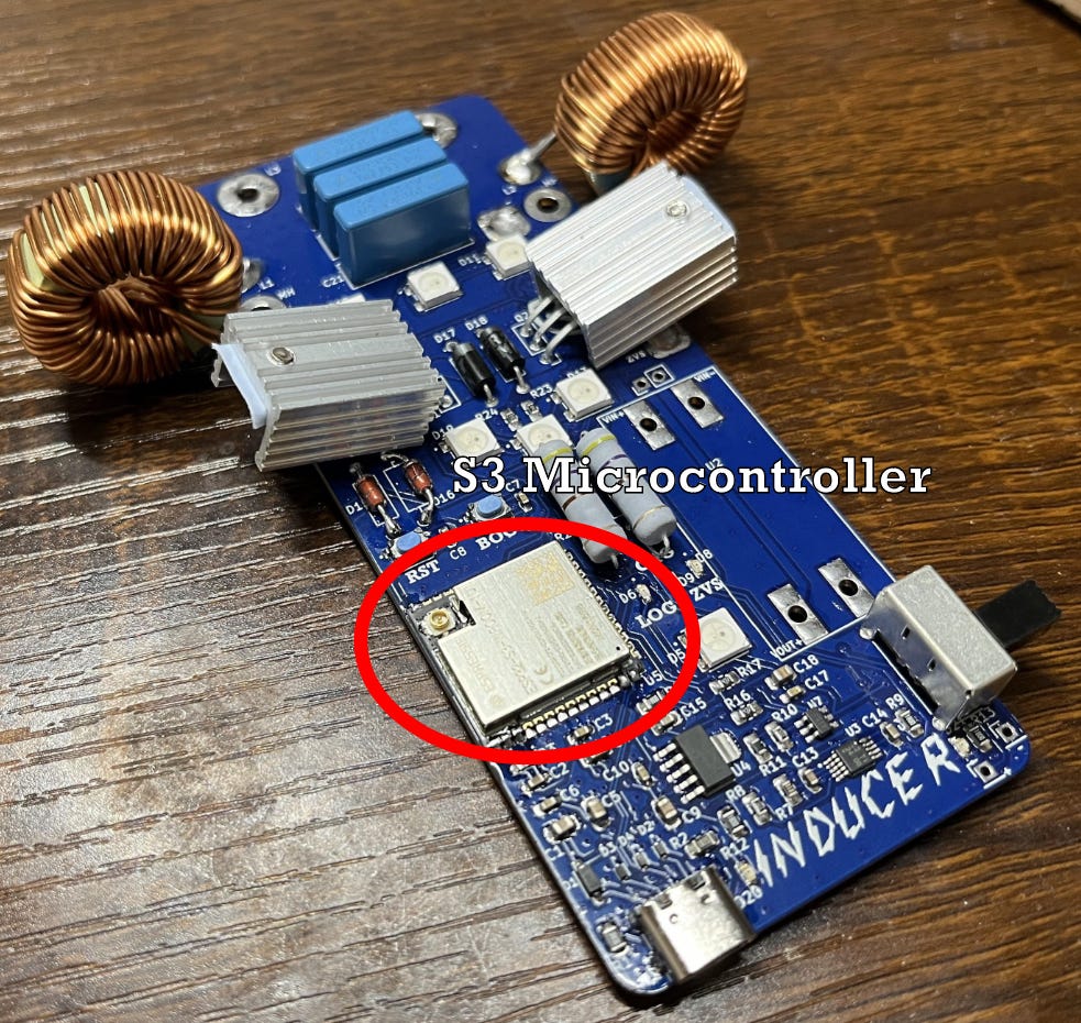
*The PCB from my Inducer project.
Having this already assembled for you makes for much fewer mistakes than if you were to personally design a full microcontroller while dealing with all of the complex circuitry of the ICs inside the module.

The insides of an ESP32-S3 module.
The other method is the SOC way, which is basically what I just said but the opposite. This is for more complex board designers to assemble the perfect PCB, dealing with all of the fragile components that would normally already be in the proper places inside the module. Some really good designers such as Maker Moekoe make projects like this. This is a great way to step up your game, however, I definitely don’t recommend it if you’re doing it for the first time. There are far too many mistakes that could be made!

*Maker Moekoe’s Picoclick C3.
Let’s go ahead and move forward with the module method.
The Schematic
First, we need to put together the ESP32-S3 and C3 schematics. I normally use KiCad for this since it is a free and pretty amazing software. However, others also work. The first microcontroller we will look at will be the ESP32-S3.

To acquire the schematics for this microcontroller, all I did was search for the datasheet. There are normally separate datasheets for the different components (module, SOC, DevKit, etc.) so the one we want to look at is the one that interfaces the WROOM/module with the other components. This would be the DevKit datasheet.

Then scroll down to the schematic.

Upon the click, we should be looking at something like this:

Don’t freak out! I know it looks like a lot, but we don’t need to interface all of it. Let me explain.
If we look over the “general” ESP32-S3 Series datasheet, and scroll down we can see that the ESP32-S3 chip supports USB communication and even gives us the pins for the USB lines.


This means we can completely bypass the USB-to-UART IC in the schematic, which honestly looks like the most complex part.

Much better! Plus, as you get more advanced in electronics you’ll see that integrating other ICs into your projects really isn’t so bad, but for now, let’s just keep moving on with our new/simpler schematic.
With this done, we can just go ahead and copy the parts into our KiCad schematic! It is also allowed to switch up the components per your specific PCB application, although this new schematic gives a nice general guideline. For example, although you don’t need to keep the Zener diodes (LESD5s) and protection diode (1N5819) on the USB lines for most applications (to protect whatever you plug the board into), I like to keep them there anyway for extra protection. Also, when integrating ICs into your schematic, SnapEDA is a fantastic resource for downloading free IC footprints and schematic symbols.

This is the USB-C adaptation since the original schematic uses Micro USB. The added 5.1k pull-downs are for communicating power draw with your computer (USB-C thing).
Another example would be the voltage regulator, which steps down the 5V from USB to a safe 3.3V for the microcontroller. In the schematic, an SGM2212-3.3 IC was used but we can switch it out for a more popular AMS1117-3.3 instead. Or if you need to power the microcontroller off of a LiPo battery, you can use any other LDO (low drop-out voltage) regulator. All you would need to do to change it is to check the datasheet for that part/regulator and copy over the application/example circuit to your preferences.
AMS1117:
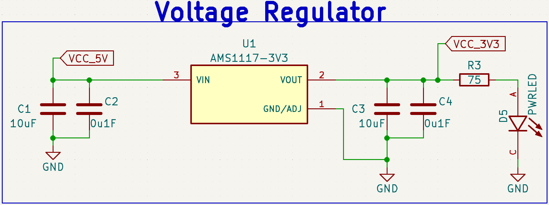
The AMS1117 is basically the same setup as the original. Notice I also added an optional power indicator LED.
LDO:

However, you should always look through the datasheet before copying anything in case there is anything specific you need to add to get a certain function. The “Typical Application Circuit” is just a good outline.
If you’re ever in doubt about how you should decouple a power line, it’s (generally) a good rule of thumb to use a 10uF and 0.1uF/100nF capacitor in parallel since they will cover a large range of frequencies. This is good for smoothening out the voltages of any unwanted noise/spikes.
Now we can just copy over everything else from the datasheet. This should be your result:

For a higher-quality image, feel free to open the image in a new tab.
Look familiar? It should! This is the general schematic I use in all of my projects.
After that, we can do the same thing for the ESP32-C3 (which also supports USB).

For a higher-quality image, feel free to open the image in a new tab. If you’re wondering why everything has a (2) after it now, it’s because I made both of these on the same schematic page and needed to separate the connections.
In some exciting news, I was also able to resolve a small but annoying bug (or possibly feature) that was not spoken about in the datasheet schematics. Whenever you first turn on your ESP32-XX board, most of the time you need to press the reset (RST) button in order to get the board going. This can be super inconvenient in situations when you may not have easy access to the button such as when it’s in a 3D-printed enclosure. I was able to resolve this by adding 10K pull-ups to the BOOT/RST lines. Surprisingly, this bug is also in a lot of commercial DevKits which I always found annoying. It’s not a huge issue, but a nice one to have resolved now nonetheless.

That’s it for the schematics!
Designing the Board
Now that we have the circuit, it’s time to put it together on an actual PCB. I’ve always found that this is like an art to PCB designers since everyone has a different style.

Step one is the layout. After assigning all of your components in the schematic a footprint (SnapEDA is your friend), you need to outline the board shape. It could be a circular board, rectangular, or other weird shape.
*Weird shape.
After that, import everything from the schematic to the PCB. In KiCad, this can be done with the button below. Just make sure everything is assigned a footprint or it won’t appear in the layout! The editable KiCad files I used for this project can be found in this post for paid subscribers.

Then, while referencing your schematic, start grouping the different components on the layout. You’ll want to ensure that components like capacitors are as close as possible to the IC they’ll be connecting to for the best performance. You’ll also want to do your best to try and line up a general path for when you start routing traces such as below (but don’t actually start routing yet).

You can see how the components are lined up in a way to easily route the VCC_5V later.
Once you’re done, you should hopefully have something similar to the one below. Feel free to also try and make it look nice or even put some text on there.
NOTE: I’ll only reference photos from the ESP32-C3 layout for now to keep things simpler. However, you should use the strategies I show you on the C3 for the S3 and all your boards!

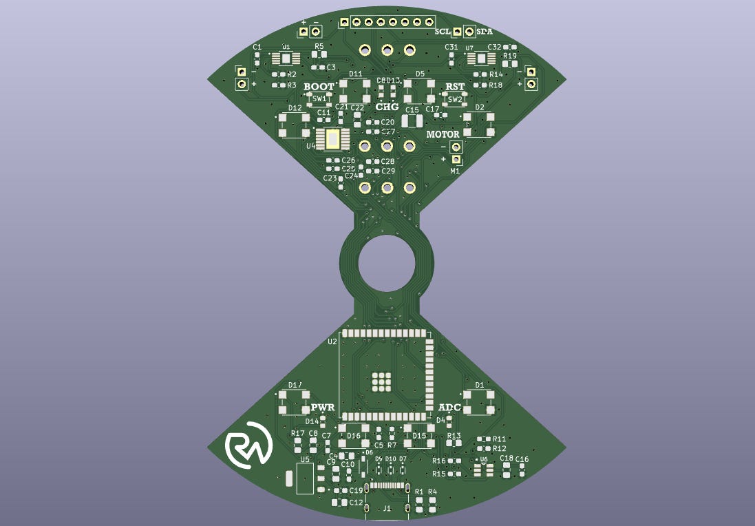
ESP32-C3 layout.
With this done, it’s time to get routing! It should be noted that this is for a two-layer board.
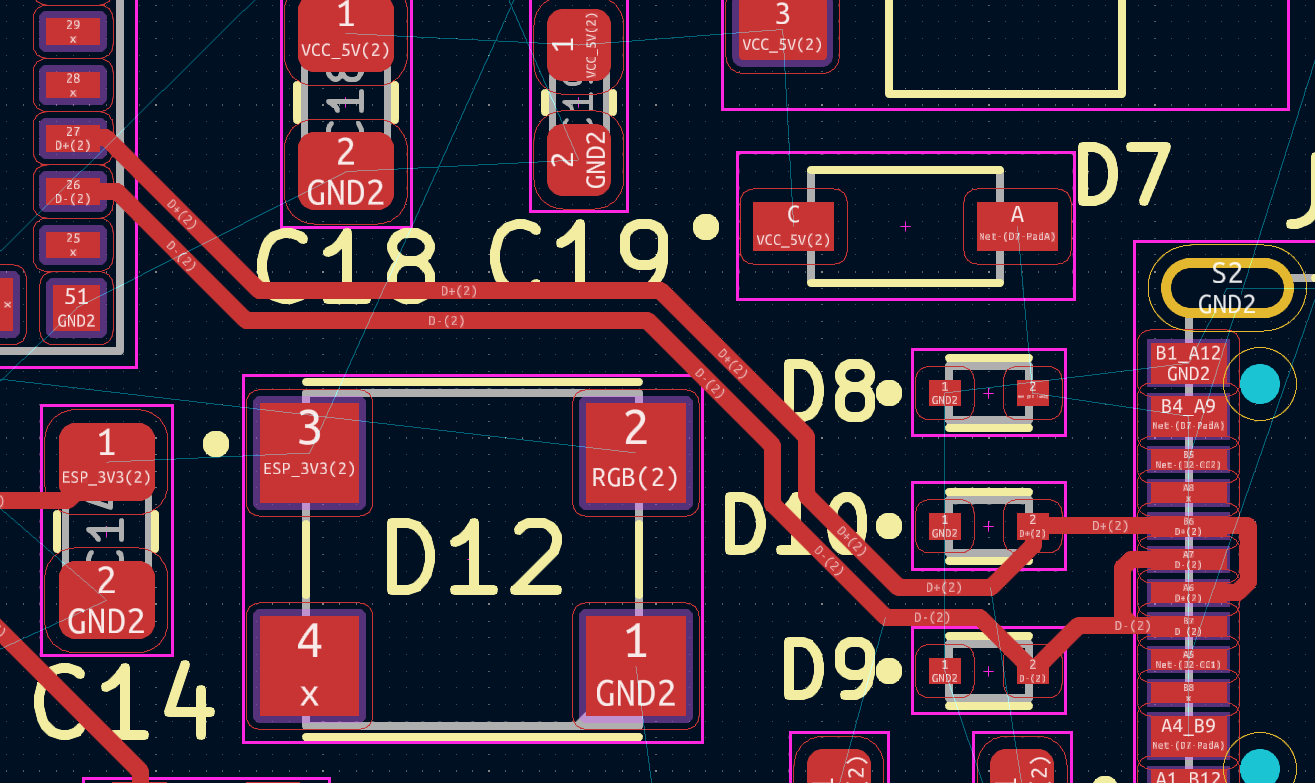
The very first thing I like to route are the USB D+ and D- lines. They are the most important traces because your board is as good as garbage if you’re unable to upload any code. It is important to route these traces as a differential pair, meaning they need to be as close as possible to each other and about the same length. This will make more sense if you watch the video below which nicely explains USB protocol.
Step 3:
It should look something like below when you’re done. It is also not a terrible idea to always leave some space around these traces and try your best to avoid routing any analog signals too close.
After that, you can work on routing the rest just by following the connections the software instructs you to!
You can also connect vias (the white and yellow circles) to any traces you need so that you can go under the top layer traces and help them reach their destinations better. Just be sure to try to keep this to a minimum! You want the vast majority of connections to be on the top layer.

For handling ALL ground connections, just break a trace slightly away from the pad and connect a via to the end. This is because later, we will fill the PCB with a ground plane which will automatically connect to all the ground vias and provide nice coupling and isolation to the rest of the board.

*Just like this.
After some time, you should have most of the connections done.
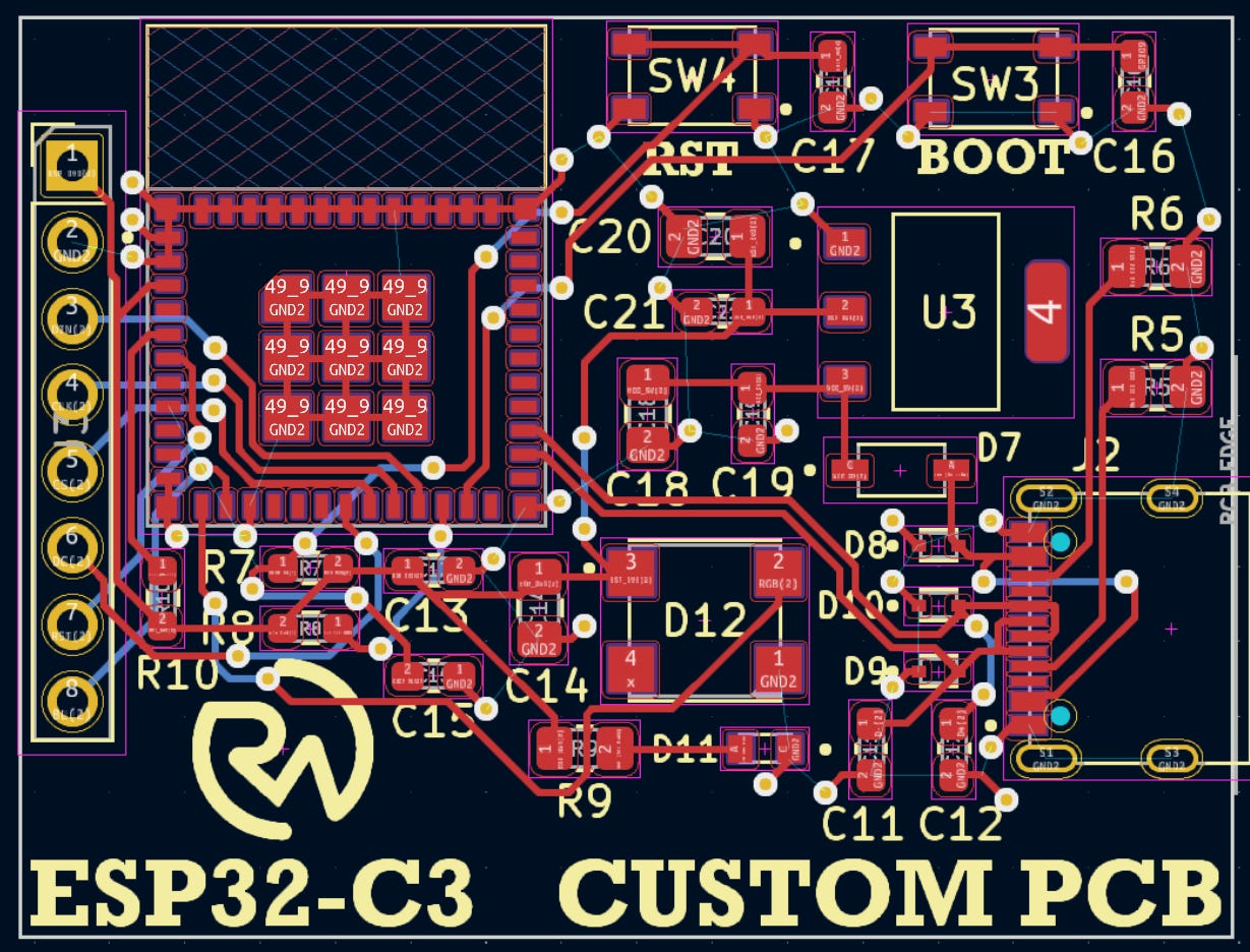
*Connections for the ESP32-C3.
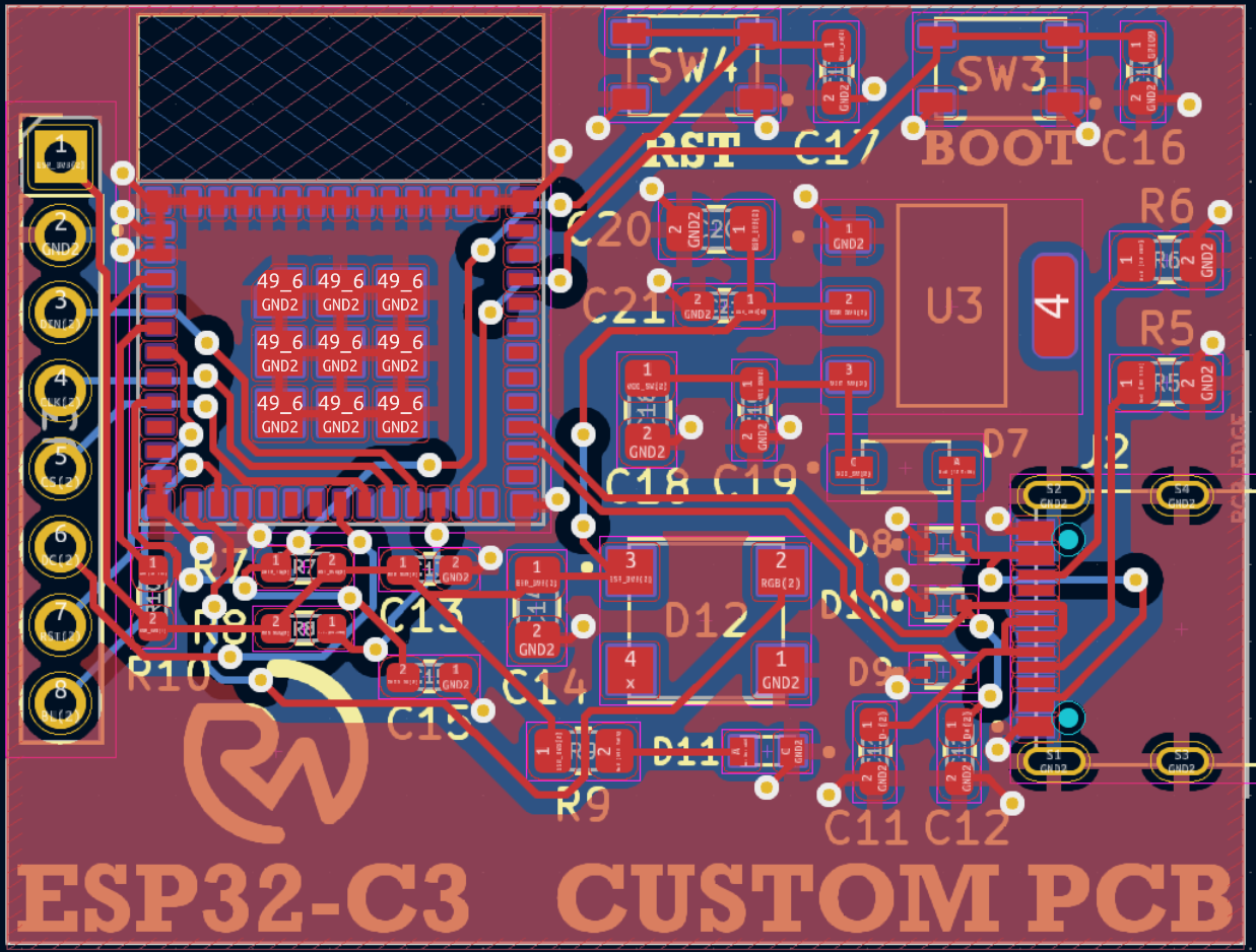
To fill in the rest, it’s time for the ground plane. Just select “copper zone”, click the two layers, ground net, and fill it in!

*You should also have your settings set to remove islands! (I have two grounds because I am making two boards at once, you should only have one.)
You should get something that looks like this at first, with some areas on the top or bottom not filled in because there was nowhere for the layer to connect to them.
This is okay! We’ll fix it later. It’s not a huge problem that this happens and many designers just ignore it (which is fine), however by fixing it the board gets better ground coupling and reduces the EMI. Here’s a great video if you want to learn more.
Step 4:
With the ground plane connecting up the vias, it should become pretty easy to see what still needs to be connected. You can also run a DRC (Design Rules Check) to see if you’re missing anything. You will probably get a lot of errors, but that’s okay for now.

Once that's done and I’ve ensured everything is connected, I like to place down some extra ground vias all around. This fills in the gaps I was talking about earlier in addition to connecting up the planes and providing more adequate thermal relief. It’s one of those “can’t hurt” things.

*It should be noted that I added R14 and R13 in this photo to help with automatic booting.
With this, we’re almost done! Time to go back to the DRC and clean up all the errors.

You’ll probably see a lot of errors for clearance, hole sizes, thermal, and unconnected ends. This is okay! A lot of the clearance ones can be ignored, especially any that may be between holes and pads on already pre-made footprints. The only ones you need to correct are any that you placed. After adjusting them, you should be in good shape.

For any hole size/“drill out of range” errors, it’s important to check with your manufacturer. At PCBWay, the minimum is 0.2mm so you can ignore any errors that are or are above that size.

For any “track has unconnected end" errors, you should just click on them and delete them manually. For any thermal errors, they can be easily fixed by adding some extra traces going out.

For anything else, you can always feel free to check the KiCad forums. Chances are high that other people have experienced the same problem and will walk you through it. In addition, if you ever get sick of seeing the same error that you know isn’t an actual error, you can always change the board settings to reflect that of your favorite PCB manufacturer.

If you’re wondering what that weird thing is in between the two PCBs, they’re mouse bites! It’s a cool technique I found to make it easy to produce multiple boards in one go. If you’re interested, the footprint I used can be found here. Once the boards arrive, you can use them to easily break them apart into two perfectly good PCBs.

It should be noted though, that you should really make a frame and connect them better if you do any more than two PCBs or if they’re smaller. Here’s a great video that can walk you through the process in addition to some other strategies such as V-scoring.
Step 5:
Once you’ve checked all the errors and are happy with the PCB, you can export it! We will want to do this as a Gerber file, which is the standard for PCB manufacturing.
In KiCad, you can export it by going to file > fabrication outputs > Gerbers.

After that, we can plot it and generate the drill files. If you want to have assembly done for you or have a higher-end stack-up, you can also generate the map file. However, this is not needed for most hobby boards.


Then, just go to your files and compress them all into a zip. This zip file is what you’ll upload to get your boards made!

Plus, as an optional step, you can also check your Gerber file in the Gerber Viewer to make sure that everything was exported correctly.The Gerber file I made for this project can be found here.
Assembly
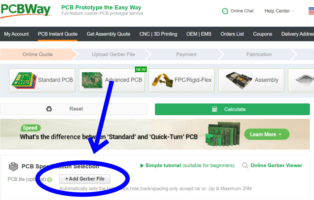
Now, it’s time to get those beautiful new boards ordered! As usual, PCBWay was my go-to.

They provide super high-quality PCB fabrication services, in addition to some other awesome things like 3D printing (even in metal) and CNC services. For KiCad users (like myself), you can even skip all of the Gerber file steps by downloading the PCBWay KiCad plug-in. It’s awesome, you just click the button and you’re done.
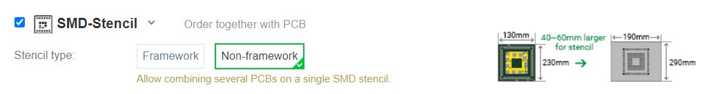
However, you can always just order through their website by going to PCBWay.com, clicking on quick-order PCB, and uploading the Gerber/Fab file link for the board. Or alternatively, just go here which I have saved in my favorites bar. I recommend clicking the stencil option at checkout to save some headaches!
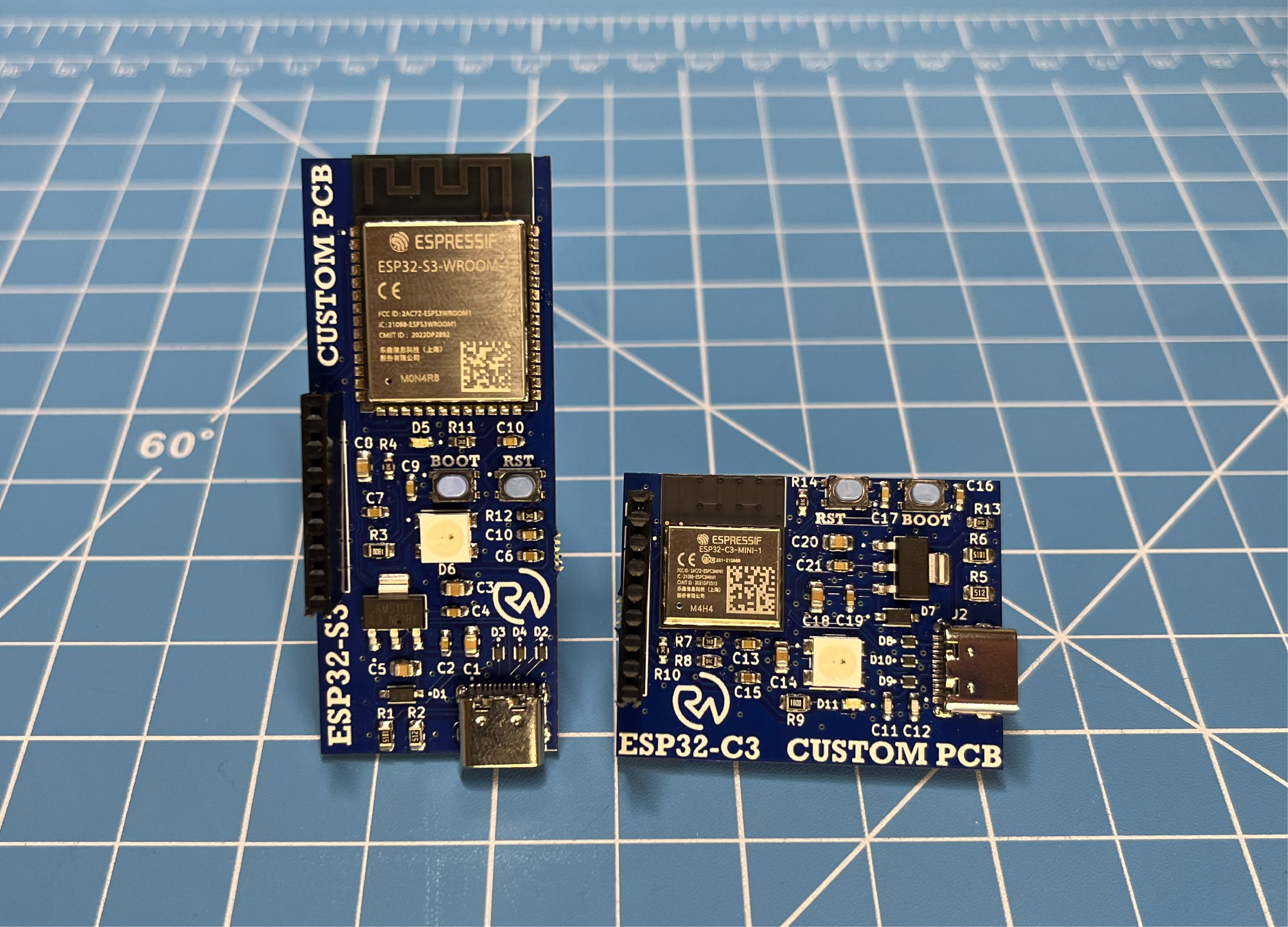
The boards were as beautiful as always when they arrived a few days later.
![]()

Now let’s assemble them!
The part list with all of the SMD components that you’ll need can be found here.
The reference/placement sheet needed to identify where to place all of the components on the BOM can be found here.
Here’s a quick video to walk you through the process:
Step 6:
Hopefully, yours should look something like below:

Beautiful! After this, you shouldn’t need the stencil anymore so you can go ahead and break the PCBs apart. You can do this with your hands or some pliers.
If the left-over bit bugs you, you can also sand it off.
Once that’s done, you’re done! Congratulations on making a successful microcontroller board! It sure is amazing how much processing can fit into such a small area.

But this is just pretty hardware right now. Let’s test it by connecting it up to a 2-in, colored display. I recommend soldering on some female pin headers to make the connections easier.

After that, you can just line up the display’s pins and push it in. All the pins are already lined up for you, so you don’t have to do anything else. I am using a Waveshare 2-inch IPS LCD Module for this.

![]()
It’s pretty funny to look at the ESP32-C3 board with the display head-on, since the board is so small you actually can’t even see it behind the display.

To get the displays working, it’s time to program these puppies! Unlike I usually do, I’m going to go into a bit more detail on how to set them up in the Arduino IDE. This way, anyone doing this for the first time can set these up with confidence.
But before I do, I would like to give a big shout-out to Soldered Electronics for supporting my work! They were kind enough to send me some awesome storage lockers and other goodies for my ever-increasing supply of components, which play a big part in me not losing all my stuff while building these awesome projects.


They have a huge variety of kits and components to help teach you about the amazing world of electronics and are an awesome shop for makers. Plus, if you think the TFT display I’m using for this project is cool, Soldered has high-resolution Inkplates up to 9.7 inches across! I really appreciate Soldered Electronics for helping support my work and definitely recommend you check them out when building your next project. Now, let’s get programming!
Programming
First, let me walk you through how to set up ESP32s on the Arduino IDE. Great guides like this one already exist, but basically, all you do is Install Arduino IDE > File > Preferences > Additional boards manager URL > and paste “https://raw.githubusercontent.com/espressif/arduino-esp32/gh-pages/package_esp32_index.json.” Then, you can go to the boards manager and install ESP32 by Espressif Systems.

With that, you can go to the top and search for your board. You will want to select the “Dev Module” of your ESP32 board. This would be the “ESP32C3 Dev Module” for the ESP32-C3 and the “ESP32S3 Dev Module” for the ESP32-S3.

Then just choose the port you plugged the board into and upload the code!
It should be noted that the Arduino code is the same for both, but you will need to change the User_Setup.h file depending on the display you’re using and the pins you’re connecting. If you’re using the same display as me, you’re all set! But if not, you’ll need to adjust the settings.
- If you’re uploading to the ESP32-C3, you will need this User_Setup.h file.
- If you’re uploading to the ESP32-S3, you will need this User_Setup.h file.
To change the User_Setup.h file, all you need to do is go to where the Arduino libraries are stored on your computer > click on TFT_eSPI > click on User_Setup.h > then delete everything and paste in the code linked above depending on which board you are uploading to (the C3 or S3). Don’t forget to save with Ctrl+S! (You can do this in Notepad.)

This code defines the settings for the TFT display you are using, such as the driver, color settings, resolution, etc. The only reason the code is different for the C3 and S3 is that different pins were used to connect up the TFT display. Besides that, everything is the same because the display is the same.

Again, you don’t have to do anything here if you just copied the code I linked! This is just for reference if you want to use TFT displays in future projects.
With that, click upload on your Arduino code and watch your display come to life using the hardware you built!

The demo that I used is just an example from the TFT_eSPI library, but if you want to learn more about how you can use the TFT display, there are plenty more for you to check out! This one even shows you how to upload custom PNG images.
BOM
This is the Bill of Materials for my ESP32-S3 and ESP32-C3 microcontroller project!
I’ll put everything that you need to have here so that you don’t have to go scrolling around looking for the links I sprinkled throughout the article.
- PCB (this is the Gerber file)
- Part list for the PCB
- Placement/reference sheet (for assembling the PCB)
- Waveshare 2-inch IPS LCD Module (colored TFT display)
- Female pin headers
- Optional (if you don’t already have them):
- Solder
- Soldering iron (Pinecil is awesome)!
- Solder paste
Disclosure: These are affiliate links. I get a portion of product sales at no extra cost to you.
Thanks so much for reading! I hope this was a helpful and informative article. If you decide to do the build, please feel free to leave any questions in the comments below. If not, I hope you were still able to enjoy reading and learn something new!
Have constructive criticism? I’m always looking to improve my work. Leave it in the comments! Until next time.
Be sure to follow me on Instagram! :)
If you feel I’ve given you at least $5 worth of information through my articles, please consider becoming a paid subscriber on my homepage. I don’t use ads, so I rely on your support to keep going! You will also receive the following benefits.

![Tim's Mechanical Spider Leg [LU9685-20CU]](https://content.instructables.com/FFB/5R4I/LVKZ6G6R/FFB5R4ILVKZ6G6R.png?auto=webp&crop=1.2%3A1&frame=1&width=306)


