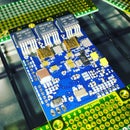
Introduction: DIY Prototype Printed Circuit Board (PCB) Manufacture
I have built a number of projects that required PCBs to work as well as they do, I produced a number of boards for my Ultimaker 3D Printer project and I thought I would document the process of making PCBs from scratch! For the prototype stage I manufactured the boards myself as it would have been too costly to send the board designs to be professionally manufactured on a one off basis. I produced the boards myself using these basic techniques and was able to save a substantial cost whilst ending up with a good end result.
Step 1: Circuit Board CAD Design
The first stage of manufacture was to design the board layout using a CAD package. I chose to use Eagle CAD which has a free version that was appropriate for my needs and is very popular within the maker community, I also have used it in the past so was pretty fluent in its operation and feature set. I created schematics of the basic circuit which I then routed into a board file.
Step 2: Board Layout
The next stage of the design process was to convert the circuit diagrams to a board layout that could be transferred to copper clad fibreglass circuit board. The software allowed me to see which pins needed to be connected to each part, this made it easier to ensure the correct electrical connections were being made. I always try to make board single sided to enable a simplified manufacture workflow, however because the switches were on the top of the board and the Arduino was on the bottom I needed to solder on both sides. I could have used SMD tact switches but I already had a load of through hole ones I wanted to use.
Step 3: Stencil Printing
After the computer design stage the Pads, Vias and Top layers were exported from Eagle for single sided boards and an extra Bottom layer for the double sided boards. The artwork was then mirrored and printed on to clear acetate sheet; I printed two copy’s so 2 sheets could be layered on top to eliminate and light leaks that could happen because of uneven toner coverage.
I got the acetate sheet from WHSmiths in the UK, you can buy it online too.
Step 4: UV Exposure
I then cut the photo sensitive copper clad board to a size just larger than the acetate artwork which was then affixed to the photoresist side of the board with tape after removing the black protective film the circuit board. It was important to do this in a darkened room to prevent unwanted exposure. The board was then placed in the UV exposure unit for about 15 minutes to sensitise the area where there were no traces or pads.
Step 5: Developing
After being exposed, the boards needed to be developed, this is done using a strong alkaline solution such as 1% diluted sodium hydroxide. However I had better success using a Seno developer which I bought in an applicator bottle similar to a shoe polish container with a sponge pad on the end. This made it much easier to develop areas of the board in a more localised way as I found using the sodium hydroxide solution created uneven results.
Step 6: Etching
After successfully developing the boards the traces and pads turned a green colour which could then be used as an etch resist. Green parts would stay copper and anything not green would be etched away, leaving just the fibreglass board remaining. The etching process is fairly easy but involves some hazardous chemicals and needs to be handled carefully. I used Clear PCB Etchant from Mega Electronics which is a relatively safe etchant but takes a little longer than Ferric Chloride which is the traditional choice and is stronger. However the clear is much less toxic and does not stain clothing. It comes in a powder which requires mixing with hot water to make a solution for etching PC boards. Once a solution is made up, the board can be submerged and the etchant will start removing the copper in the un-masked parts of the board. A small PCB usually takes about 30 minutes for the etchant to fully remove the unwanted copper, I found rubbing the board using an old toothbrush helped to speed the process up.
Step 7: Special Treatments
The last stage was to finish the board by removing the etch resist with isopropanol alcohol or nail polish remover, this then exposes the shiny copper which can be soldered to straight away or finished with a solder mask. I bought a tube of green UV curable solder mask online relatively cheaply. This requires a similar process to the photo etch method to apply the mask to the board. Another product that could be used was Liquid Tin which coats the copper traces and pads with a very thin layer of tin which helps with the soldering process and stops the coper oxidising.


