Introduction: TI's BMS Analog Frontend Module
Designing PCB for TI's BMS Analog Frontend: Schematic Design, layout, PCB design, PCB fabrication
Step 1: Introduction
A Battery Management System (BMS) is an electronic system that monitors and manages rechargeable batteries, ensuring safety, efficiency, and longevity. It oversees parameters such as voltage, current, temperature, and state of charge, optimizing battery performance and preventing issues like overcharging or over-discharging. BMS is crucial in various applications, from electric vehicles to renewable energy storage, ensuring reliable and safe operation of battery packs. In this project, we're designing a PCB for the analog front end of a Battery Management System (BMS) utilizing the BQ76930 voltage sensing IC.
Attachments
Step 2: Components Required
Step 3: Schematic Design
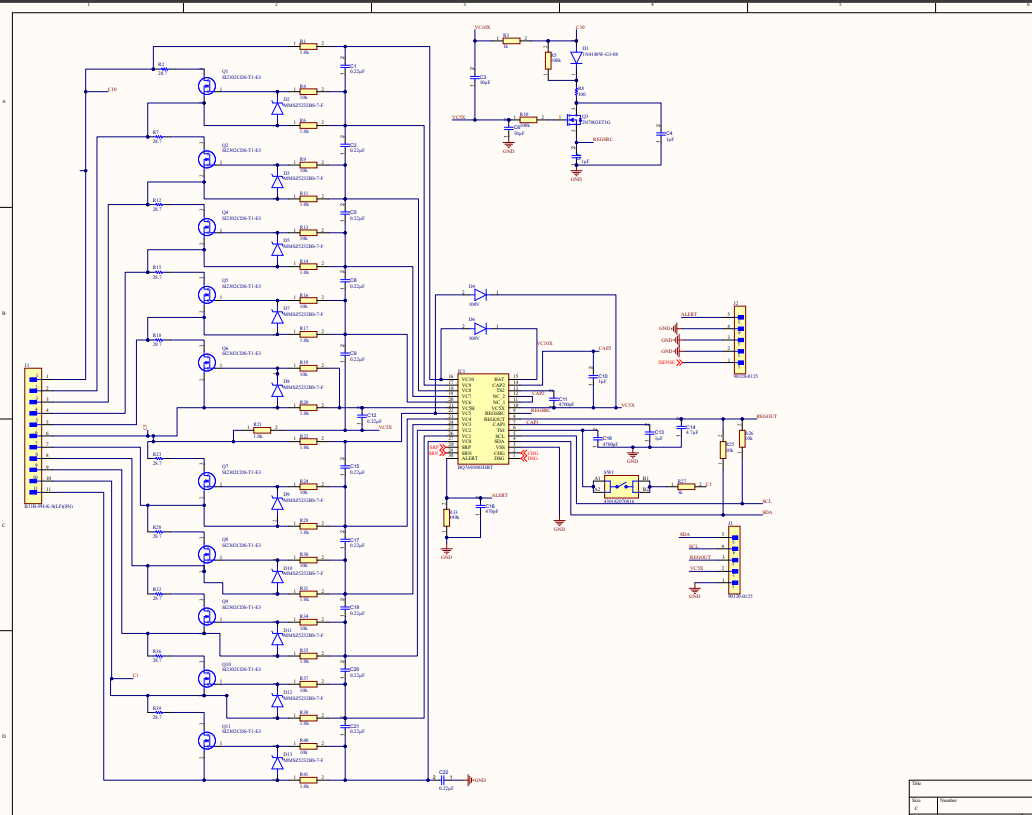
The schematic for the Analog front end can be obtained at TI's official site or you could go to the below site
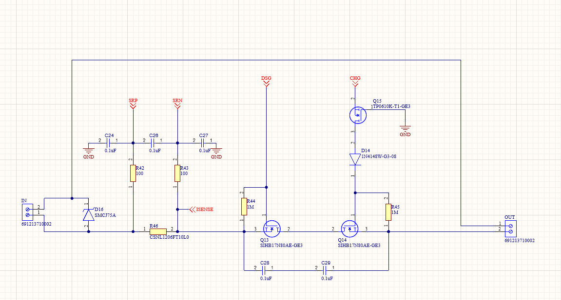
Create a schematic file in Altium and design the schematic for the stack connection of 10S2P having only an analog front end. If you want to solder the components on your own then you should change the size of some of the components according to your ability to solder them. Also, keep in mind the power requirements of all the components because the size of the components depends on their power.
Step 4: PCB Design
Initiate a new PCB document in Altium, then navigate to Design > Update Schematics in BMS.PrjPcb. After importing all modifications, create the layout in Altium. Establish connections using traces to link air wires. For guidance on routing in Altium, refer to the instructional video provided below.
Upon completing the PCB design, generate Gerber files for manufacturing. Navigate to File > Fabrication Outputs > Gerber Files, customize settings, and then proceed. For drill files, go to File > Fabrication Outputs > NC Drill Files. Access the Generated (Gerber) folder, double-click any file, and choose Explore. In the file explorer, select all Gerber files, create a zip file, and save.
Step 5: PCB Printing
Steps to Order Your JLCPCB:
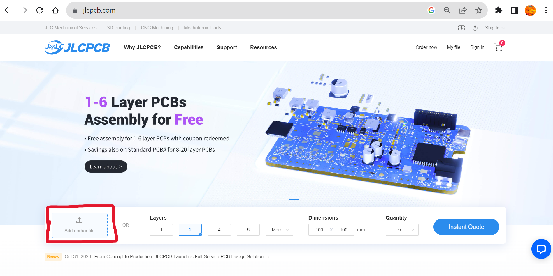
Now equipped with the completed PCB design, the next step is to procure the printed circuit boards (PCBs). Head over to JLCPCB's website https://jlcpcb.com/HAR and initiate the process by clicking on the "QUOTE NOW" button.
JLCPCB, a generous sponsor of this project, stands out as the largest PCB prototype enterprise in China, specializing in swift PCB prototyping and small-batch production.
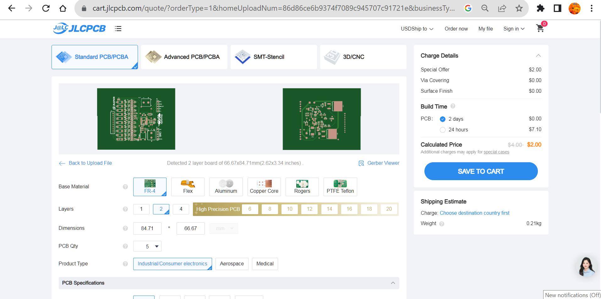
With JLCPCB, you can order a minimum of 5 PCBs for a remarkably low cost of $2. Simply upload the Gerber file obtained in the preceding step, either as a .zip file or through drag-and-drop. Upon successful upload, a confirmation message will appear. Verify the PCB design using the Gerber viewer, examining both the top and bottom views.
Once satisfied, proceed to place the order at an exceptionally reasonable price point—$2 for 5 PCBs. If it's your initial order, benefit from an even more attractive offer of 10 PCBs for $2. Click on "SAVE TO CART" to finalize the order.
In my experience, JLCPCB's manufacturing process was swift, taking only 2 days, and the DHL delivery option ensured that the PCBs arrived within a week. The packaging was secure, and the delivered PCBs exhibited commendable quality, meeting the expectations of this project's requirements.


