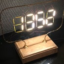
Introduction: PCB Prototyping With Verowire
There are many ways to prototype a circuit board, the most popular include the traditional Solderless "Breadboard" where components and wires can be plugged in to spring terminals in a plastic base. When a more permanent circuit is required it is common to use strip-board which is a single or double-sided PCB with perforated tracks pre-installed. By bridging and cutting the tracks it is possible to create boards of some complexity. This board is generically known as "Vero board" named after the originator of the system described in this instructable.
A third form of solder proto-board is Perfboard, also known as Dot-board which is similar to stripboard but the pads are not joined and circuits are constructed by soldering on individual wires or bending the leads of through-hole components into the right places.
Back in the early days of computing it was common to use Wire-Wrap to assemble computer boards as there are no real limits to the routing of the conductors and multi-layer circuit boards were not yet common. As each wire is individually insulated they can lie against each other with little penalty which allows very free routing.
The "Verowire" technique combines aspects of wire-wrap with solder proto-board techniques using Perfboard as the substrate.
Step 1: Equipment
The Verowire system consists of a special dispenser for enamelled copper wire. This is available from (amongst other sources) RS Components where is has part-number 105-4626. For many projects this is all that is needed, but for more complex layouts plastic combs are available to help organise the wires and divert them around the board.
The wire is of the "self-fluxing" type which means that the insulation can be readily soldered-through. Wire where this is not the case would make the process impossible.
Step 2: Lay Out the Board and Components
Decide where the components will go on the board. The picture shows an Arduino shield being constructed, which is why the upper set of pins have had their retainer removed to bend an offset into them. This is a recycled bit of perfboard, which is why it has some missing pads and oversized holes. The components need to be held in place either by bending pins or by soldering pins that will not be used. It is difficult to Verowire to soldered pins, though it is possible to solder temporarily, desolder with a solder-sucker them and then wire with the enamelled wire.
Step 3: Start to Wire the Components.
Start by pulling an inch or so of wire out of the dispenser. Hold this down to the board (or over the edge of the board) and wrap tightly around the first pin using the dispenser. The dispenser has a sliding friction brake which can be used to hold the wire when wrapping or released when moving to the next location. It can also be slid back and then forwards to push out a little slack, which often makes wrapping a pin easier. Squeeze the slider to pull the wrap tight around the pin so that it stays in place.
The combs fit in to the holes in the board. They can be glued, but this is not normally necessary.
I tend to wrap about half a dozen terminations at a time before soldering them as a batch. The extra wire length can be snipped off with side-cutters either before or after soldering. Every time I make a Verowire board I promise myself that I will buy some cutting tweezers, but I so far never have.
It takes some time for the solder to melt the insulation and for the pad to "run". The pads also tend to end up a bit blobby. As far as I can tell that is just the way it is, you will just have to temporarily lower your standards.
Step 4: Surface Mount
This process is clearly not really intended for surface mount components, but they can be incorporated if required. The trick is to pre-tin the end of a wire and stuff it down a hole, lay the component on the pad and then solder. This works best adjacent to component pins where one end of the SMT can be soldered to the pin-pad first.
Step 5: Check the Board
This method is prone to short-circuits between adjacent pads if the wire is not cut off short enough. It is also relatively easy, if the iron moves on too quickly, to cast an insulated wire into the solder blob and not have any continuity, so the board must be checked both for shorts and bad joints.
Step 6: Summary
This method is not suitable for every application, but it is particularly useful when a lot of tracks need to run around the board and cross each other. The board illustrated used more than 100 pads and quite a complex routing, it would have been very difficult with strip-board and not trivial with a real PCB.
Re-routing is relatively easy, in general the bad traces can just be cut back to a convenient point and left in place when a new trace is wired.
I suspect that this method would have too much cross-talk for high-frequency applications.
I don't know what the maximum sensible voltage is for such a board. The wire has a proof voltage of 600V and is rated for 100mA. In this board which has a 90V line I ran a conventional length of wire for that track.


