

Introduction: Arduino DCF77 Analyzer Clock MK2


See my site for this clock Arduino DCF77 Analyzer Clock Site
This Clock displays the DCF77 time code on 2 rings of 60 LEDs on a large 12" (305mm) diameter dial. The inner ring shows the live time code for the next minute as it is received and the outer ring shows the current time as long as the previous minute was received error free.
A further 24 LEDs show decoder status and time info. Decoded time and date are shown on 2 large 8 digit 7 segment displays while DCF77 pulse timings and bit information are shown on a further 2 smaller 8 digit 7 segment displays.
The clock uses 2 x Atmega 328 microprocessors (Arduino Uno) , 1 to control the DCF77 Analyzer and 1 to control a Udo Klein Super Filter. The Super Filter allows advanced DCF77 signal processing and also tuning of the Arduino quartz crytal. The filter is switchable and has 10 status LEDs to show the state of signal reception and quality of output. The clock also chimes the hours, quarter hours and seconds tick through 2 off JQ6500 sound modules.
Most of the electronics are mounted on the rear of the dial so the clock can be fitted to many differnt case styles.
I have included designs for a retro and modern style clock cases. the retro desgn is fitted into an old dial clock case while the modern design is fited into a black picture frame.
Step 1: Credit


This clock is based on the DCF77 Analyzer Clock by Erik de Ruiter and is an updated version of my Mk1 DCF77 Analyzer clock.
Pic 01 above Erik de Ruiter's DCF77 Analyzer Clock pic 2 my MK1 DCF77 analyzer clock.
Erik has provided full details of his clock here on GitHub See pictures of his clock here Flickr and Arduino Project Hub .
Differences between Eric's Clock and my clock
Although based on Eric's clock I have made a few changes to the hardware. Please mix and match whatever option suits your needs but make sure you change the code to suit.
I use two custom made Arduino UNo's on the Veroboard rather than a Uno and a Mega.
I use cheap 7 segment displays and dot matrix modules from China throughout and have changed the code to match. See the section on display errors as they work really well once these mods are carried out.
I use 2x JQ6500 modules rather than the Adafruit sound board. As one of my boards is software controlled there are some software changes and another library to load.
As I have a Arduino Uno instead of a Arduino Mega I do not have all the spare pins to drive the decoder LEDs so I use a 3rd dot matrix module instead.
I have modified Udo Klein's Super Filter by adding extra staus LED's. The brightness of these LEDs are PWM controlled by the DCF77 decoder Uno via 2 transistors not the Super Filter Uno.
There is also an LED test function added to the Super Filter to match the DCF77 decoder test funtion.
I only use 3mm LEDs and have chosen matched brightness LEDs to try and keep the brightness uniform.
I have added 4 seperate intensity levels in software so the Ring/Status LEDs, the large 7 segment displays, the small 7 segment diplays and the Super Filter LEDs all have custom brightness levels depending on the readings from the single LDR.
I don't have a temperature or week number display on my clock and have modified the code to suit.
I have added extra monitor LEDs to my Super Filter so on my clock there is only an option for Sythesized and Non Sythesized output. This is no option to switch modes as per Erik's clock.
The DCF77 Sound on my clock has been modified to accentuate the differnce between the incomming 0s and 1s. When the clock detects a 1 it just plays a slightly longer sound than 200mS.
Step 2: Video
Video 1
The video shows the clock running with the tick sound on and also the clock chimimg the full quarter and the hour.
It also shows the dial layout and informatin on reading the displays.
Video 2
This video shows the clock power up, display test and time decoding.
Video 3
Show how the Udo Klein Super Filter works on my DCF77 Analyzer.
Video 4
Picture frame version. The video shows the clock running with the tick sound on and also the clock chimimg the full quarter and the hour. It also shows the dial layout and informatin on reading the displays.
Video 5
This short video shows my DCF77 analyzer clock displaying and decoding the DCF77 signal. All sounds are off bar the DCF77 live signal.
Step 3: Dial LEDs


Pic 1 DCF77 Filter and DCF77 Status LEDs
Pic 2 Inner and outer ring LEDs
Pic 3 7 segment displays
Step 4: Controls


The clock is controlled by 7 switches that are mounted on a metal bar. The switches are attached to the inside of a hinged door that folds down under the clock for access.
On the picture frame version the switches are fitted to a cutout on the side of the clock.
Switches controll the following
Tick sound On/Off
Tick Volume
Chime 24/7 or timer
Chime Volume
DCF77 sound On/Off
Reset Super filter or Analyzer
DCF77 Source from Filter, Off or Analyzer
Switch Functions
Tick Sound Turns the tick tock sound On and Off (removes power from the JQ6500 module)
Tick Volume non locking Turns the tick tock volume up and down (Tick sound switch must be On)
Chime Control Off chimes are turned off 24/7 chimes are on 24/7 Timer chimes are only on at set times of the day e.g. off at night
Chime Volume non locking Up turns volume up Down turns volume down After each button press a test chime is played so you can hear the new volume setting
DCF77 Sound On plays the DCF77 sound being received as beeps through the Piezoelectric sounder. 0 being 100mS and 1 played as a 500mS beep to make it easier to differentiate the received 0 & 1s. Off the DCF77 beep sound is Off
Reset non locking Filter resets the DCF77 Super Filter making it re-sync to the DCF77 signal Analyzer resets the DCF77 Analyzer starting with a display test if enabled and then a clock re-sync. RTC time will be displayed from the time stored in the real time clock
DCF77 Source Off disconnects the DCF77 signal from the clock Analyzer the DCF77 signal is fed direct to the clock without any filtering Filter the DCF77 signal is taken from the Super Filter and if the Super Filter is synchronized this signal is synthesized to the correct error free signal
Step 5: Schematics


There are 3 schematics for this clock. The main board, the dot matrix modules and the 7 segment display modules.
The 2nd is very large for and can be viewed full size here 4000x4000 schematic. I have laid it out this way to make it easy to wire.
Step 6: Atmega Pin Connections


This clock uses 2 Atmega 328 ICs on custom vero Boards. A standard UNO can be used for the Analyzer part of the clock but a UNO with a quartz crytal rather than a resonator must be used for the Super Filter part of the clock.
The first 2 pics show the pin outs for the 2 ICs with chart 3 showing how these translate to the Arduino IDE.
Step 7: Vero Board Layouts


Many of the modules for this project are pre-built and just need to be plugged in but the main board for the Arduinos, sound modules and 3rd LED Matrix need to be built on Vero board.
Pictures 1 & 2 show the main board. The LEDs are shown mounted on the board for reference only.
All wiring to other boards from the main board is via PCB header connectors. The connections from the main board to the switch panel is directly wired. This allows the main board and switch panel to be removed for maintenance.
Note these are configured as Arduino UNOs and while prebuilt Unos or Nanoscould be used the Super Filter Arduino has to have a quartz crystal not a resonator for accuracy.
See the info on my Master Clock site Arduino quartz crystal modification
Pictures 3 & 4 show the JQ6500 module board.
Pictures 4 & 6 show the common connections board for the 3rd LED matrix. The RTC is mounted here but only connected by the header cable.
Step 8: Pre-built Modules


Pre-built board and modules
Pic 01
LM2596 Regulator Module drops the voltage down to 5v. This is adjusted by the 10K preset resistor on the module and measured after the revearse protection diode D4. Adjust this before adding the Arduinos to the board.
Pic 02 & 03
RTC DS3231 I2C
This module stores the time from the decoded DCF77 signal. The built in clock has temperature compensation and has battery backup in case of power failure. Note the RTC module is modified to take non rechargeble batteries.
Pic 04
MAX2719 Dot Matrix Module
These modules drive the inner and outer LED rings (2 modules) and the 3rd module drives all the other LEDs bar the Super Filter LEDs. The LED matrix is removed and a PCB header soldered in place.
Pic 05
RCWL 0516 Doppler Radar Sensor Microwave
To turn the clock displays on only when the room is occupied I use motion detection. You have a choice between the RCWL 0516 below that will detect movement from behind glass or the PIR module below.
Pic 06
PIR Module Infrared
The PIR module can be used instead of the Doppler Radar Sensor above. The drawback of this device is it can not be used behind glass or perspex etc.
Pic 07
Max2719 7 Segment Display 0.56"
This is the larger 0.56" version used for the the time and date display. I had a batch of these already but there are similar modules on tindie. Just make sure you are getting the larger 0.56" displays Note a small modification may be required to prevent display errors on thes modules. See the MAX2719 modification step.
Pic 08
Max2719 7 Segment Display 0.39"
This is the smaller 0.39" version used for the the bit, error and pulse displays. They are available all over eBay and Amazon just make sure you get the modules with the header pins not soldered or the boards with the pins soldered to the back of the module. Note a small modification may be required to prevent display errors on thes modules. See the MAX2719 modification step.
Pic 09
JQ6500 16p Modules
One of these modules are used to play the ticking sound and the other the quarter and hour chimes. With the sound files included with project you should be able to get away with the cheapest 16p mosdule with 2M of memory. The modules drive a single 3W 8Ω speaker each. Sounds are loaded from your PC (not MAC) via USB using a simple program.
Step 9: LEDs


I used Vishay TLH44 series High Efficiency LEDs in a Ø 3 mm Tinted Diffused Package
DESCRIPTION The TLH.44.. series was developed for standard applications like general indicating and lighting purposes. It is housed in a 3 mm tinted diffused plastic package. The wide viewing angle of these devices provides a high on-off contrast.
Several selection types with different luminous intensities are offered. All LEDs are categorized in luminous intensity groups. That allows users to assemble LEDs with uniform appearance.
FEATURES
• Standard Ø 3 mm (T-1) package
• Small mechanical tolerances
• Suitable for DC and high peak current
• Wide viewing angle
Pic 1-4 show the LED colours with pic 5 showing the chart with the actual part numbers.
Step 10: DCF77 Receiver

Pic 1 my DCF77 Receiver Module from http://www.pvelectronics.co.uk
These items don't seem to be available anymore but try Amazon
PV Electronics DCF77 Receiver Module connections Connections from left to right
1.VDD 2.TCON 3.PON 4.GND 5.NC
Provides output in an inverted format (output is low, and goes high once per second).
Low power standby mode - connect PON to Vdd.
Connect PON to GND for normal operation.
Keep the receiver well away from TVs, monitors or any other electrical noise and make sure it points at the DFC77 transmitter.
Step 11: Power Supply


The clock uses around 450mA max with LEDs at full brightness and drops down to around 80mA with the displays off.
You should be safe with a 1000mA DC PSU from 7 -12volts (the onboard module controls the voltage)
Pics 1 & 2 I use a common PSU with 10 battery backed up fuses and 8 non backed up fuses to power all my clocks.
I always fit fuses to my projects as this PSU can put out 10 amps. The individual 2amp fuses in the PSU panel cover the cabling to my projects and I then fit a smaller fuse in my projects.
Step 12: Wiring Order

With around 400 odd wires to connect the wiring needs a lot of planning in order to fit the wiring runs in the gaps between the modules.
Buiild modify if required and fix all boards to the rear of the dial so the wiring harness runs are visible.
The dot matrix boards are removed and wired away from the clock.
Wire the Super Filter LEDs and fit into the dial.
Wire the DCF77 Status LEDs and fit into the dial.
The Super Filter and DCF77 Status LEDs are connected by header cables to the main board. Wire all the LEDs on dot matrix module 3 and fit into the dial.
Wire from dot matrix module 3 to the small breakout vero board and then wire away to the LEDs for this module fitted in the step above.
Wire the outer LED ring and then fit into the dial.
Wire the outer ring dot matrix display leaving the wire ends long enough to terminate on the outer ring LEDs.
Re-fit the outer ring dot matrix display and terminate the wiring harness to the outer ring LEDs.
Wire the inner LED ring and then fit into the dial.
Wire the inner ring dot matrix display leaving the wire ends long enough to terminate on the inner ring LEDs.
Re-fit the inner ring dot matrix display and terminate the wiring harness to the inner ring LEDs.
Wire all the LEDs on dot matrix module 3 and fit into the dial.
Wire from dot matrix module 3 to the small breakout vero board and then wire away to the LEDs for this module fitted in the step above.
Build header cables and connect to all boards.
Fit main Vero Board and then wire to the switch panel. The LDR is mounted through the hinged wooden door the switch panel is fixed to so this is wired at the same time.
Fit speakers and connect to the Vero Board with the JQ6500 sound modules.
pic01
If you have drilled the correct sized holes in the dial all the LEDs will push fit into place with no glue. Make sure the inner edges of the LED holes are coated with paint/varnish in the painting stage to help with the friction fit.
Step 13: Wiring Max2719 Dot Matrix Module Modification


pic1
Before wires can be connected to the MAX 2917 matrix modules they will need to be modified.
Remove the Dot Matrix LEDs as these are not required.
pic2
Two sets of 8 90° pin connectors will to be soldered to the lower edge of the existing LED matrix connector.
pic3
Modified MAX7219 module with 90° pin connectors soldered in place to the bottom of the old LED Matrix connectors.
Wires are taken away from these points to the LED matrix on the main board.
pic4
Side view showing the pins soldered to the side of the old LED Matrix connector pins just above the PCB.
Step 14: Wiring Building a Wiring Jig


The jig will hold the LEDs in place with the correct spacing allowing easy wiring away from the clock.
Building a wiring Jig for the LEDs
pic01
Print out the dial onto a sheet of paper. Print in reverse or lay the paper back to front as you will be working from the rear of the clock. Lay the sheet on an old bit of wood or melamine. Center punch all LED centers and drill with a 3mm drill bit. The hole should be a friction fit on the LEDs to ensure easy wiring. LEDs differ in diameter so do a few test holes first to get the correct size for your LEDs.
pic02
Completed wiring jig.
pic03
Completed Inner & Outer LED rings on the jig. It may be handy to write the LED numbers and other info on the jig to ensure you wire the correct LEDs as the LEDs are fitted to the rear of the dial and are reveared/go anti-clockwise.
pic04
Ring of LEDs removed from the jig ready for inserting into the dial.
Step 15: Wiring LED Inner and Outer Ring


The schematic diagram pic 1 above shows the wiring for a section of 8 LEDs of the outer LED ring..
First push the eight LEDs into the holes in the jig. Bend all the anodes so they connect together as per the shematic and solder in place. A wire is connected to the eight connected anodes from the LED matrix module later. Fit a small bit of insulation sleeve over the cathodes then bend these legs around 15mm from the LED. Cut around 5mm from the bend and solder a short length of wire long enough to reach to the next batch of eight LEDs. See pic2.
Pic 3 show a completed section of 8 LEDs wired on the jig with wires leading away to the next section of 8 LEDs.
Pic 4 Repeat the process above in batches of eight LEDs.
Each batch of eight LEDs will have it's own seperate anode connection to the dot matrix module. Eight in total.
Pic 5 Outer ring LEDs completed along with the 16 wires connected to the dot matrix display.
The LEDs are then pushed into the holes in the dial and the matrix module is fixed back onto the dial. Once in place the 16 wires from the dot matrix module are connected to the outer ring LEDs. This process is repeated for the inner LED ring.
Pic 6 This is part of the schematic for the picture above.
The 16 wires from the dot matrix module are ready to be connected across the 8 sets of 8 LED sections. Note the 8th set has only 4 LEDs. The full sized 4000x4000 schematic can be seen here.
Step 16: Wiring 3rd Dot Matrix Module

Wiring the 3rd Dot Matrix module
This module has only 24 LEDs connected out of 64.
The day of the week LEDs on the 1st section of 8 LEDs (only 7 connected)
The 2nd of 8 LEDs are CEST,CET Leap Yr,RTC Error,Synced, Error Period and Error Pulse Width (only 7 connected)
The 3rd of 8 LEDs are Buffer Full, Parity 3 to 1 pass and fail and Buffer Oveflow (all 8 LEDs connected)
The 4th of 8 LEDs just contains 2 LEDs Minute marker and DCF77 Status
I could have just used 3 sets of 8 LEDs but using 4 sets made wiring simpler.
These LEDs are wired on the wiring jig then conected to a small Vero board where they are connected to the Matrix wires. Note this board also acts as a mount for the RTC.
Step 17: Wiring Switch Panel


Pic 01
The switch panel swings down under the clock fixed to the back of the access door. The wiring is soldered direct to the main board and includes the wiring for the LDR.
Pic 02
Switch panel
Pic 03
Switch panel wiring in progress
Pic 04
Switch panel with completed wiring loom
Pic 05
Completed wiring with the wiring loom for the switches snaking down from the main board.
Step 18: Chime and Tick Tock Sounds on the JQ6500


Pics 1 & 2 This clock uses 2 x JQ6500 modules one for the tick tock sound and one for the quarter and hour chimes. The tick tock sound is hardware controlled and the chimes are software controlled.
Chime Circuit Pic 3
Switch SW7 is a 3 position locking switch. The module is controlled over serial hardware pins 13 & 14 on the Arduino. Note the 1K resistor on the receive circuit. See main schematic. Off - power is removed from the JQ9500 and the 24/7 /timer pin is held high to prevent the Arduino pin from being left floating 24/7 - The chime will sound the four quarters and the hours 24/7 Timed - The four quarter and hour chimes will only sound from 05:15 untill 23:00 hrs. (set in code) The volume is set in software via the Arduino and the Chime Volume up or down switch.
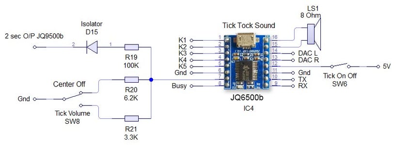
Tick Tock Circuit Pic 4
This is hardware controlled direct to the JQ6500 Switch SW6 Tick On/Off just removes the power from the JQ6500. Tick volume SW8 is a 3 way center locking switch. Operating the switch up or down sets the volume via the ADKey pin on the JQ6500. The command to play the tick tock sound arrives every 2 seconds from the Arduino. The sound file must be less than 2 seconds. Diode D15 isolates the ADKey from the Arduino output.
Step 19: Speakers


Speakers pic 1
The sound modules are each connected to an 3W 8Ω speaker attached to the side of the clock case. These are available as a pair from Amazon.
Pic 2 Shows the speaker locations in the clock case. Note the folded up switch control panel in the bottom of the clock.
Pic 3 2 speaker grills cover the speakers and were also from Amazon
Pic4 Left side of clock showing speaker location. This is repeated on the other side.
Pic5 Picture frame style clock showing the right hand speaker.
Step 20: JQ6500 Loading Sound Files


Your sounds will need to be loaded onto the JQ6500 module.
See these sites for info and Arduino libreries for these modules.
Arduino Library JQ6500_SerialGeneral infoJQ6500 tools
Normally the JQ6500 come preloaded with a music uploader program that loads on connection to your PC (won't work on MACs!) . This is in Chinese there are instructions on my site here showing how to use the Chinese version.
My JQ6500s came without a loader program so I downloaded an English version from Nikolai Radke
You can get the zip file from here English Language MusicDownload.exe v1.2a
I just run this file from windows (no need to install it) and it runs in English see details below.
Insert your JQ6500 into PC via USB.
Pic 1 When the file is run this window will open. Click FILES
Pic 2 Click CHOSE FILES and shift select all the files you want to be copied to the module. Note rename the files for the chimes as below.
1 to 12 are the hour chimes. 13 to 16 are the quater chimes and 17 is the test chime used when setting the chime volume using the Chime Volume Switch.
Pic 2 Click OPEN above then click on the FLASH tab PIC 3.
Click on FLASH pic 3 and you should get a message saying FILE PROCESSING It the files will fit on the module the message will change to FLASHING RUN and a green bar will show progress.
When flashing is completed the message will change to READY......
You can remove your module and plug it into sound board on the clock.
Repeat this for the Tick Tock sound (1 file this time) on the 2nd module.
Sound files are enclosed. I mixed these sound files up on Audacity pic 4 at 48KHz sample rate the max quality the JG6500 board can handle. The chimes were mixed on multiple channels to get the real harmonics then mixed back down to a single channel for the JQ6500.

Step 21: JQ6500 Library Modification

Modify the JQ6500_Serial.cpp file in your Arduino libray folder
Using the standard library every time a chime is played the library waits in case there is a reponse. This wait causes the clock run out of sync and any received data errors until the next minute.
I found this on google and is a reply from the author of the library. ~~~~~~~~~~~~~~~~~~~~~~~~~~~~~~~~~~~~~~~~~~~~~~~~~~~~~~~~~~~~ Before sending a command, the library waits for up to 10ms to see if there is any left over data from the device... https://github.com/sleemanj/JQ6500_Serial/blob/ma... after sending the command the library waits for a response for up to 1000ms
https://github.com/sleemanj/JQ6500_Serial/blob/ma... and after that it will wait at least 150ms while reading the response
https://github.com/sleemanj/JQ6500_Serial/blob/ma... since in the case of playFileByIndexNumber you don't need a response at all
https://github.com/sleemanj/JQ6500_Serial/blob/ma... you could perhaps get away with adding if(!responseBuffer && !bufferLength) return;immediately after the last command byte is written (currently line 263 of JQ6500_Serial.cpp)
https://github.com/sleemanj/JQ6500_Serial/blob/ma... that should reduce the time required to about 10-20ms probably.
~~~~~~~~~~~~~~~~~~~~~~~~~~~~~~~~~~~~~~~~~~~~~~~~~~~~~~~~~~~~~~~~~~~~
After adding the line after line 263 if(!responseBuffer && !bufferLength) return; the clock worked fine.
Step 22: Modify the Real Time Clock RTC


Modification of DS3231 AT24C32 I2C Precision Real Time Clock Module
My clock uses a DS3231 AT24C32 I2C Precision Real Time Clock Module.
The module comes supplied with a Lithium-Ion rechargeable battery see pic 1. I use a non rechargeable battery so have removed resistor R5 from the module as pic 2.
Pic 3 Location of R5 on the DS3231 module.
Pic 4 Charging Resistor R5 removed (just scrape it off).
Step 23: Dial Construction Drawing


Pics 1 & 2
The dial requires oround 700 seperate drilling operations and numerous aounts of cutting and filling to complete.
I don't have a CNC machine so it was all done by hand. The dial was drawn up on a Cad program (TurboCab) pic 4 and printed out onto injet water slide decal paper.
Pic 3 Shows a close up of dial printing with 3mm LEDs to give an idea of scale. The quality from the water slide decal paper is very good far better than my old ink jet can print.
The enclosed zip file contains the dial picture in various file formats including 2 4000x4000 png files one for printing the dial and one showing all the layers including cut outs.
Contact me for other file types!
Attachments
Step 24: Dial Construction Cutting Out & Drilling


Pic 1 The dial is cut from 1.5mm thick alluminium sheet as it has to carry the weight of all the electronics and wiring.
Pic 2 Make a template by printing out the dial from your CAD program onto A3 paper.Make sure it has center marks for the LED holes and also the cutouts for the 7 segment LED displays.
Pic 3 Carefully cutout the 7 segment display openings on the template with a craft knife.Place the template on the alluminium sheet and tape it down to stop it moving. Center punch all the center marks for the LEDs and draw around the openings for the 7 segment displays with a marker pen.
Pic 4 Remove the template to reveal the cutting/drilling marks on the alluminium sheets protective film.
Pic 5 Draw a circle the size of your dial with a compass using the center punch mark from the DCF77 symbel LED as a center point.
Pic 6 Cut out the circle with a hacksaw/jigsaw or bandsaw fitted with a metal cutting blade.
Pic 7 Cut out the 7 segment display openings with a coping/jig or fret saw. Take your time with this as it will save a lot of filing later.
Pic 8 Drill out all the holes for the LEDs. I start with a 1mm bit then a 2mm and then finally a 3mm bit.
This leaves the LEDs a friction fit once the paint and varnish is applied to the dial.
Pic 9 Mark center punch and drill 3 or 4 dial mounting holes.
Pic 10 With the holes drilled the protective film can be removed from the alluminium sheet and the dial rubbed down to remove all rough edges.
This will also give a good key for the paint.
Pic 11 Prime and paint with acrylic paint then a coat of matt varnish. Antique White looks better on old dials or use pure white on modern dials.
Step 25: Dial Construction Applying the Dial Transfer Decal


Pic 1
Water slide decals are printed out on special paper on an inkjet printer. Once dry they are soaked in water then slid into place.
They give a very detailed print and once given a coat of varnish are tough. Don't forget to order transparent tranfers so the dial colour can be seen through the transfer. Follow the instructions with the pack as they do vary.
On my transfers I print out the dial on transfer paper let it dry and then cut it out to just under the size of the dial. I then give it a coat of acrylic varnish. When the varnish is dry the transfer is soaked in water until the transparent transfer comes away from the white backing sheet.
Pic 2 Line up the transfer with the dial and slide it over the dial.
Pic 3 Make sure the center dots line up with the center of the holes in the dial then slide the backing sheet back off the transfer.
Pic 4 Carry out any final adjustments then remove any airbubbles.
Allow to dry then apply some clear acrylic varnish to project the transfer. Once this dries carfully cut away the transfer around the 7 segment display cutouts with a craft knife. Then cut the transfer off all the LEDs hole. I used a leather punch just smaller than the hole. Give it another coat of varnish to seal all the cut edges Leave it overnight to dry.
Pic 5 Search for "Transparent Water Slide Decal Paper A3"
Step 26: Dial Construction PCB/Vero Board Mounts


The PCBs and Vero Boards are fixed to wooden mounting blocks cut from off cuts of timber.These block are glued to the dial with impact adhesive. Follow the instructions on the impact adhesive but normaly you apply to both surfaces leave until tacky then press together for an instant bond that hardens fully over night.
Pic 2 Lower modules in position on the wooden blocks ready to be secured by M2 screws.The main PCB fits on top of the lower 7 segment modules and is raised up on brackets.
Pic 3 JQ6500 sound module board and LED wiring board in place. RTC is mounted on the LED wiring board but connected on the main board.
Pic 4 Main board mounted on custom made standoff brackets.
Step 27: Dial Surround & Back Box Restoration


Dial Surround Restoration
I sourced my clock case from eBay. It had no dial or brass bezal and the rear box was broken.
Pic 1 The original Oak dial surround was covered in a thick coat of varnish and years of dirt.
Pic 2 I used paint stripper to remove the varnish and then wood bleach to get rid of the very dark areas of wood.
Pic 3 The surround was then varnished with matt acrylic to enhance the grain of the wood.
Pic 4 The back box was very badly damaged and had to be screwed and glued back together. I has to fill many hole and cracks in the wood work and decided to paint it matt black.
Step 28: Correcting MAX7219 7 Segment Module Display Errors


The 7 segment modules seem to work fine work fine on their own. However, once you start daisy chaining them together the displays tend to error.
Pic 1 0.39" Display
Pic 2 & 3 The datasheet calls for a 10μF and 0.1μ capacitor across the supply rails as close to the MAX7219 as possible.I notice the 0.1μF capacitor is in place but the 10μF capacitor is missing.
Add this capacitor in the 2 holes above the diode D1 on the rear of the display.
Pic 2 & 3 There is also a diode in series with the supply rail. When daisy chaining modules all these diodes are in series so the further down the line of modules the more volts are dropped causing display errors.
Remove this diode on each display and replace it with a wire strap.
Pic 4 0.56" Display Note the black tape over the 3rd and 6th digit tp make colons.
Pic 5 A 10μF capacitor added to the rear of the PCB on the +&- pins of the MAX7219 IC
Pic 6 The 1N4148 diode is replaced by a wire link.
Step 29: Increasing the Constrast on the 7 Segment Modules

The 7 segment displays traditionally would have a sheet of red perspex to match the LED colour placed over the top of the display. This was designed to hide the not lit segments and provide contrast to the LED segments that are on.
In my clock I have used Neutral Density Heat Proof Dimming Transparent Acetate Sheet ND 0.9.
This hide the not lit LED segments and provides the contrast needed in bright conditions. It has the advantage that it work on all colour LEDs.
My 0.56" modules are a deeper red than the 0.39" modules so I would need 2 different matching red perspex to sheets to work well on both modules.
The acetae shhet is also very cheap the only disadvantage is that it is too flimsy to cover large areas without support.
Pic 1 shows the effect of the ND sheet. The lit LED segements have more contrast and the unlit LED segments are hidden. It also hides the black tape masking for the colon display.
Step 30: Modification of the RTC Time 7 Segment Display Module to Show Colon Digit Seperators


Pic 1 The standard display only has decimal points to separate the digits and has no colon that would normally be used in a clock display.
Pic 2 in code I have set digits 3 and 6 to always display a "o" lower case o
Pic 3 Black plastic tape is then cut with a craft knife and placed over the 2 digits leaving a small section showing
Pic 4 When the display is on these visible sections now display colons
Step 31: Dial & Case Fitting


Pic 1 & 2 The dial is hidden behind a brass bezal. The brass bezal was missing from my clock but i was able to get one from a horological supplier.
Pic 3 the brass bezal is held down by a brass catch set into the dial surround.
Pic 4 with the brass bezal removed you can see the recess cut in the surround for the brass bezal hidge. My new bezal hinge was a differnet shape to the original hinge so I had to cut it in with a chisle at the front and fill the rear in with a piece of wood stained to match the surround.
Pic 5 This shows the dial with all the LEDs and display removed.
Pic 6 The dial has been removed showing the dial mounting holes on the wood surround and the wooden back box behind it.
Pic 7 Shows the surround removed revealing the back box construction. The switch panel can be seen folded up above the trap door in the base of the back box.
Pic 8 Shows the side view of the case with dial and wood dial surround locked in place. The dial surround is locked by the same type of catch used to lock the brass bezal in place. Note the small brass screw below the brass tag on the dial bezal. this ensurse the brass bezal lines up correctly with the dial when the brass bezal is closed.
Step 32: Dial & Case Fitting Modern Style Case and Surround


Pic 1 This case uses a large picture frame with a basic square back box to hold the electronics and to hold the dial away from the wall to give it some depth.
Pic 2 Outer frame and glass removed to reveal the thick photomount card over the dial (a thin ply or wood sheet can also be used with a routed edge)
Pic 3 Photo mount removed to show how the dial is fixed to the back plate with 4 small screws.
Pic 4 The backplate holds the dial and has a large circular cutout for the electronics.
Pic 5 It is hinged at one edge to the dial can swing out.
Pic 6 The speakers are mounted on both sides with holes and grills as per the other case.
Pic 7 The switches are mounted on the side in a cutout with the speaker grill above.
Step 33: DCF77 Filter


DCF77 Filter
When switched on the Udo Klein's Super Filter actively processes the incoming DCF77 signal from the antenna/receiver. After a few minutes of sampling the DCF77 signal the Super Filter will predict the DCF77 signal and use this to determine if the incoming signal contains any errors. The Super Filter will then synthesize a corrected DCF77 signal even if the signal is absent.
Pic 1 Super Filter Mod See the schematic I have modified the Super Filter Code to add extra monitor LEDs. In order to do this I have removed 4 modes from the filter just leaving sythesized and inverted sythesized.
Note the PWM LED brightness control is via the Arduino controlling the DCF77 decoding not the Super Filter Arduino. I have also added an LED test to the Super Filter to Match the LED Test on the main clock. This activates on reset or power up. On power up the Supe Filter LED test starts and finishes then the main clock LED terst starts.
Pic 2 The filter will lock onto the DCF77 signal even if the signal is really noisy. As days progress the filter uses the incomming DCF77 signal to adjust the Arduino crystal frequncy.
This means the filter will stay in time even if the DCF77 signal is lost for many days. In my clock the DCF77 signal is alway fed to the Super Filter Arduino even if the DCF77 Source switch is set to off. This allows the Super Filter to stay in sync and keep adjusting the quartz crystal from the Arduino.
Pic 3 Super Filter Monitor LEDs.
Filter On lights when the DCF77 Source switch is set to FILTER and means the Super Filter is decoding and synthesizing the DCF77 signal
DCF77 Filtered the DCF77 Synthesized signal comming out from the Super Filter
DCF77 Signal the DCF77 signal comming direct from the DCF77 receiver with no filter applied
Signal Difference the differnece between the incomming DCF77 signal and the Synthesized signal. In normal operation this will flash as the received signal shape is often slightly “wider” than the synthesized signal.
Filter Syncronized best possible quality, clock is 100% synced
Filter Locked clock driven by accurate phase, time is accurate but not all decoder stages have sufficient quality for sync
Sync Lost <200mS clock was once synced, inaccuracy below 200 ms, may re-lock if a valid phase is detected
Sync Lost >200mS clock was once synced but now may deviate more than 200 ms, must not re-lock if valid phase is detected Signal Dirtytime data available but unreliable Signal Bad waiting for good enough signal
More details on some of the above
Filter Syncronized - Timing is completely locked to DCF77 and the data is most up to date.
Filter Locked - If the quality factor of the decoder stages drops but the quality factor of the phase decoder stays high enough the clock will transition into the state locked. In this state it is still phase locked to DCF77 but it may become out of sync by a second but only if a leap second is transmitted.
Sync Lost <200mS - This indicates that the quality factor of the decoder stage and the quality factor of the phase decoder have dropped. In this state the timer relies on the quartz crystal timimgs and the clock will slowly drift out of phase with the DCF77 signal. This is a warning that the clock may be running slightly out of sync.
Sync Lost >200mS - Once the clock has started to drift out of phase for more than a set period of time (depending on the tuned accuracy of the quartz crystal) then this LED will light
Pic 4 Animation showing filter synchronized
Pic 5 Super Filter example
The top row shows the Super Filter turned on. Once synchronized and tuned into the signal the Super Filter will synthesize a good signal even when the signal is completely lost. On a noisy signal the Super Filter will search for known signal bits and keep itself synchronized to the transmitter. The bottom row shows the Super Filter turned off. Whatever signal is received (good or bad) is sent to the decoder.
Pic 6 Super Filter correcting a noisy signal as displayed on the DCF77 Scope
Normal Signal No super filter - Normal signal from the DCF77 reciever Noisy Signal No Super Filter - The aerial is moved near a LCD screen to generate noise over the signal No Signal- The aerial is disconnected and moved connected via the super filter Noise On Superfilter On- The noise is filtered out leaving a perfect signal.
Example animation pic7
Super Filter turned Off and a bad signal the clock errors and will reject this minutes data.
Note the DCF77 Filtered LED pulses as normal but as the Filter is turned off the filtered signal is not fed to the clock's decoder.
Example animation pic8
Super Filter turned On and a bad signal the clock has no errors and the clock is able to decode the data as normal.
Note the DCF77 Filtered LED pulses as normal and is fed to the clock's decoder
Step 34: DCF77 Time Code

This picture shows the dial code as it is displayed on my dial.
Step 35: Code

There are 2 seperates codes to download one for the Superfilter and one for the Analyzer part of the clock.


![Tim's Mechanical Spider Leg [LU9685-20CU]](https://content.instructables.com/FFB/5R4I/LVKZ6G6R/FFB5R4ILVKZ6G6R.png?auto=webp&crop=1.2%3A1&frame=1&width=306)


